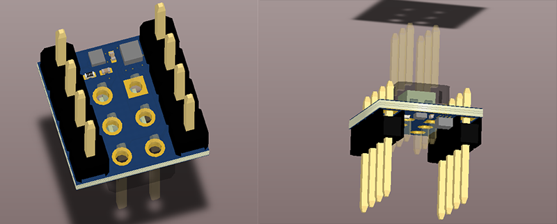
There are a few development boards entered in this year’s Hackaday Prize, and most of them cover well-tread ground with their own unique spin. There are not many FPGA dev boards entered. Whether this is because programmable logic is somehow still a dark art for solder jockeys or because the commercial offerings are ‘good enough’ is a matter of contention. [antti lukats] is doing something that no FPGA manufacturer would do, and he’s very good at it. Meet DIPSY, the FPGA that fits in the same space as an 8-pin DIP.
FPGAs are usually stuffed into huge packages – an FPGA with 100 or more pins is very common. [antti] found the world’s smallest FPGA. It’s just 1.4 x 1.4mm on a wafer-scale 16-pin BGA package. The biggest problem [antti] is going to have with this project is finding a board and assembly house that will be able to help him.
The iCE40 UltraLite isn’t a complex FPGA; there are just 1280 logic cells and 7kByte of RAM in this tiny square of programmable logic. That’s still enough for a lot of interesting stuff, and putting this into a convenient package is very interesting. The BOM for this project comes out under $5, making it ideal for experiments in programmable logic and education.
A $5 FPGA is great news, and this board might even work with the recent open source toolchain for iCE40 FPGAs. That would be amazing for anyone wanting to dip their toes into the world of programmable logic.


These tiny FPGAs are what I was talking about when I mentioned that they can be used to hide routes inside a design that is created using online tools that force you to publish your PCB designs. With a small FPGA, or three you can publish your FPGA config on github and open your board completely when you feel happy to do so and not when the site dictates.
Which is exactly a good way to declare yourself as a freeloading dick that wants to use a free service but not obey its rules. Feeling smart, Dan?
That said, these tiny FPGAs have their use – often a bit of extra glue logic next to a MCU that wouldn’t warrant a normal FPGA (or it is too large/expensive) but it doesn’t fit into a CPLD anymore.
The kind of subversive that Dan refers to is the core of being a “hacker.” To use something beyond its intended purpose is the driving force of many projects featured on Hackaday. I say give the man a medal!
You could always drop in a handful of ATtiny chips, but the FPGA is probably faster and may have analogue options.
Having people walk in your front door when they want isn’t freedom and it isn’t sharing either, opening your door to the community when you have judged that your house is in order is freedom and genuine sharing.
That is my point and it should have been obvious, unless you are a cretin, which evidently you are.
Why not just not upload your schematics / designs to the site until you’re ready in the first place? — I’m probably missing something, but If you’re not ready to share your designs, then why are you uploading them to an OSH sharing site? :-|
Also, I doubt that with only 8-pins (assuming 2 are for power/ground) you’re going to be doing much route “hiding”… would be nice if they made it a 16-PIN DIP. — I’d pay $8 – $10 for a 16-PIN DIP FPGA… — especially if it worked at 5V (or at least was 5V tolerant)…
Not really. The term of service is between the creator and the web (or otherwise) software provider. It is not a contract between the creator and the rest of the world, so the creator is not obligated to do anything.
If the provider do not specify to require firmware loads, then as long as the creator done what is required, there is no addition legal obligations and especially to 3rd parties that are not in the agreement.
FPGAs are just too expensive and also power hungry.
I often evaluated whether to use an FPGA in my designs, and the outcome was always that it would’ve saved nothing. No money, no board space, no power consumption, no design time.
They are too expensive at $1.53 each?
http://www.digikey.com/product-detail/en/ICE40UL640-SWG16ITR50/220-1961-1-ND/5155600
This is about the price that I pay for a typical mixed mode ASIC, or a medium sized 16/32 bit microcontroller. So, ways too expensive for what it offers.
And why is that relevant? I could also buy a cherry Powerade. But if a cherry Powerade won’t do the job then my manager would ask me why the hell I put in on the PCB when an FPGA or CPLD is the only thing that would work.
because it’s got what circuits crave. electrolytes.
I feel like it would be pretty rare that an FPGA or CPLD would the *only* thing that could do the job in a consumer electronics device.
An ASIC of the same size can obviously pack more logic into the same space, and run at lower power. For the smaller batches or where you might need more dynamic behavior, an MCU will almost always do. — If they’re the same price and use less power, it seems an FPGA isn’t really the right tool for the job…
The places where the FPGA wins over ASICs are mostly in the hobbyist realm — because we’re doing either small batches (usually one-offs, maybe ten-offs), and/or you are doing constant iterative development (post-development if you wanted to do a large production run, I would still recommend going with an ASIC for lower power consumption unless you absolutely needed reconfigurable computing in your product).
[Disclaimer: I’m a hobbyist, and I’m pretty excited at the prospect of cheap DIP sized FPGAs. Additionally, that I know of, I own at least one mass-produced consumer electronics device with an FPGA in it (it was designed for non-developers / non-hardware enthusiasts, and it was not a Kickstarter :-P).]
If they wouldn’t save you board space then you were looking at the wrong application for them. FPGAs are there for when there isn’t an ASIC or small number of general purpose VLSI chips to do the job.
FPGA’s are used where there is no other option other than fab an ASIC. Don’t use it for GPIO or other situations that aren’t timing critical. It sounds like you are using your own anecdote where an existing ASIC could work instead of shoehorning an FPGA one time to justify your disapproving of anyone using FPGA’s for anything. Yeah don’t use FPGAs for your passive speaker crossover or just to debounce a button.
This is – dare I say it – too small. A 16pin DIP format would be easier.
As it stands, all data needs to be clocked in and out serially.
DIP16 would be cool too, but DIP8 is still useful. I use ATtiny85s quite a bit, which are DIP8. Being small and inexpensive ( and with an open toolchain) might entice people like me who are putting off getting in to FPGAs.
Yes and I am guessing that your first code will be a serial in parallel out shift register.
These have built-in SPI/I2C primitives, so you don’t even need to build that up.
Neat.
I agree — the use case of an 8-PIN DIP FPGA seems pretty rare — for the same device if it were 16-PIN DIP, I think it would have a lot more potential!
I love the ice40 line … Great tools and powerful for thier size while fast as all hell
No config FLASH? Am I missing something. I don’t know the Lattice chips.
They have an integrated config memory.
I’ve never used them but I understand from others that they are used in hi-rel applications (space vehicles, military, etc.) because the configuration is internal.
Interesting chip. It would be interesting to create a very small CPU (like Notch’s DCPU-16 but shrunk to fit the memory constraints).
Or a single TIS-100 core.
Oh, this will eat at least the rest of my weekend.
I was wondering about something like the J1 (http://www.excamera.com/sphinx/fpga-j1.html).
Yes, am working on getting the J1 building with the iCE40 open-source toolchain.
It only has 1200 LUT’s. It’s too small, more like a large CPLD than a small FPGA.
Already exists, it’s called the mico8 http://www.latticesemi.com/Products/DesignSoftwareAndIP/IntellectualProperty/IPCore/IPCores02/Mico8.aspx
I’ve put one in a Mach XO2 640 before (granted it was assembly coded and very small code), so it should be able to fit in an ICE40
This very small AVR clone should fit http://opencores.org/project,navre
Anything that extends the currently available FPGA options is a good thing. If that $5 board can be configured as a TinyAVR with an embedded HDMI driver (say) then suddenly things start looking very interesting.
HDMI needs three differential data lines plus a differential clock. So you would need at least eight outputs. Maybe you could do the differential inverting in external logic but it would make more sense to just take a bigger FPGA with some differential I/Os.
Huh… yeah… seems like a DIP-16 would be a lot more useful… but I can’t stop thinking: “So, technically, you could do it with four outputs, and maybe some transistors and crap…? — that leaves two pins that you could use as inputs for serial IO that you could plug right into your AVR!”
Assuming of the 6 pins (of the 8-PIN DIP that are not being used for power/ground) you can configure one of them to be inputs and the other 5 to be outputs…
How small does the PCB trace/space clearance have to be to fit between the balls on the chip-scale wafer package?
At a guess, I’d say 2 or 3 thou at the largest.
Not something your typical cheap hobbyist board house will offer.
That pretty much need something like laser drilled vias & via in pad to breakout the inner balls. Either way, it won’t be cheap by the time you add in the board fab cost and assembly cost too. The final cost will be a few times the BOM.
All of that extra cost just to use a tiny part and then you have to bloat the size by sticking to dip and large header!?
BTW there might be a way to do this by throw away I/O’s. This is why it can’t be have a larger I/O counts that is suggested by other comments.
There are only 4 balls in the center, the outer ring has 12 balls. Don’t both with any of inner ones that are regular I/O. If it is a special pin like power/ground/clock/config, connect it to one of the adjacent one in the outer ring. If you are lucky that the pinout allows for this, then you can use a cheaper PCB options.
THIS is what I call “good components selection”. Amazing feat, this would open so much the world of FPGAs to newbies if this is easily programmable using cheap external stuff.
I could see a lot of prototyping possibilities for this.
I would love to play with these, and have a few projects in mind.
Anyways, this is like a perfect entry to fpgas.
IMHO, for an entry level stuff – i.e. for learning – you would be better off with e.g. one of the Papillio boards. Most of the stuff you would want an FPGA for needs a lot of I/O (memories, driving displays, etc.). This has very few pins and starting to learn about programmable logic by having to deal with SPI/I2C or something similar is not exactly easy.
Totally agree. I’m the proud owner of a Papilio Pro but from what I’ve seen so far the biggest bottleneck is the horrible Xilinx tool chain. Papilio are trying to solve this with DesignLab and while I think they’ve done an amazing job with that product it’s still nowhere near the level of accessibility that Arduino has reached with the AVrs.
I almost agree. I’ve had a original Papilio for a long time, and I’ve done very little with it. The tool chain is just so bloody huge that I can’t just start up the smart VHDL/Verilog IDE (so I can see what premade parts are available) without waiting for Xilog to load all of the “draw your design on the LUTs directly” and other routing tools that I just don’t need.
Yeah, if I knew VHDL or Verilog better I could use Notepad++, and if I knew Xilog’s offerings better I could do that and still reference the premade stuff. But we’re talking about beginners.
Ditto, The most I did with the Papilio was a couple of BCD to 7-seg decoders and counters. I probably used less than a ten-thousandth of the chips capacity.
I also agree that tying to learn VHDL (or Verilog) while trying to learn to use the Xilinx ISE is near impossible. I used Sigasi as an external code editor and that helped but still the Xilinx ISE is totally cryptic with it’s error messages.
I then went to cheap CPLD boards on ebay (breakout board with JTAG and V reg). The Altera programmer was much cheaper and the IDE was much easier to use but to be fair I had already done the basics of VHDL in Xilinx by that stage.
I should have just started with the cheap CPLD board from ebay. I would have saved myself paying about $120 for the Papilio One and LogicStart MegaWing, another $40 for a GameDuino (another false start) and $40 for the Xilinx programmer.
The Altera CPLD board was under $15 and the Altera programmer was $5-$10. So I could have started out on $25 instead of $200.
I do use the Xilinx programmer as I have been using 5V CPLD which Xilinx still make (XC9572XL). Altera also have 5V CPLD – EPM240 – EPM570 so it’s nice to have both programmers now and be able to switch back and forth between Xilinx and Altera.
The Papilio One is in the junk box somewhere, it can’t really be re-purposed because it has fixed peripherals.
The Gameduino is in the junk box to but it may make a good video output for some uC project one day.
I do agree however that this one (8 pin ICE40 breakout) is a bit too low on pin count for beginners.
Isn’t this really more a CPLD-class device with an FPGA architecture?
The Pebble Time smartwatch that Dave Jones tore down just days earlier had a similar mini FPGA, presumably as a display controller.
very nice. Just one comment, I know the connectors already look large compared to the FPGA, but I still would try to fit pads with the largest amount of copper for each pin of the connectors. Maybe use a round pad for pin-1, and square pads for all other pins? Things always fail on connectors.
there are lots of boards houses that can do it, i think more likely is finding one that can do it, and is in budget that’ll be the hard one, doing it without blind/buried via and/or multilayer. soldering that onto just pads without a place for solder balls is gonna be fun, certainly possible, but those traces are tiny, lets do it.
Holy carp, that’s a tiny package. Like an intelligent grain of salt. Wonder if it’s related to intelligent calcium:
https://www.youtube.com/watch?v=FBaVwwuErmU
These devices actually look pretty cool. Lattice also has an evalkit available:
http://www.latticesemi.com/en/Products/DevelopmentBoardsAndKits/iCE40UltraLiteBreakoutBoard.aspx
I hate to be the guy who ruins the party, but seriously? That’s an entry you actually feature? I think it’s nice that someone did a small adapter for this, however there is no “project” here. Nothing to show for really.
This is one solution of many – all depends on your goals. Sure, it’s useless for a one off project!
But it seems to be an ideal solution for something you may build 100 of. For example we are working on a smart web controlled brewery controller that has some interface logic between the web server – a Raspberry Pi – and the brewery hardware. Today that logic is taken care of with two 14 pin IC’s and one 16 pin IC and I can see where one of these might take the place of all three, reducing board size and reducing cost.
A early version of our controller is at: http://68.35.191.49.
I’m not saying there is nothing to do with a small FPGA, I used CPLDs in some of my projects and even a sub $1 device can sometimes replace 3 to 4 logic ICs – the saving in both time and money for an even small production run is there. Having that said, if you want to use the said Lattice FPGA you need to get their software write some code for it, test it using a good test bench and install in your circuit. Where does the PCB (“carrier”) comes into play?!
Quote: “test it using a good test bench”
This chip is One Time Programmable. How many times do you want to change out a 1.4mm 16 ball BGA chip on the test bench? Wouldn’t it be easier with a disposable chip carrier?
Also this thing is smaller in LUT’s than a simple CPLD. It’s more towards a System on a Chip or mixed hybrid digital analog chip.
More complete quote: “test it using a good test bench and install in your circuit”.
If you had ever worked with HDL you know that writing the test bench (https://en.wikipedia.org/wiki/Test_bench) takes place before you actually pick up a soldering iron. Also CPLDs do not have LUTs, but never mind! Point is, the actual process of integrating your FPGA into the product should be something you do only a small number of times if you know what you are doing. If you happen to find yourself in a situation where you might need to re-write portions of the code many times (doubtful with such a small device) you can simply use another device which you can re-program several times and after all is working nicely, simply install this tiny thing and you are done. The work-flow that would benefit from this so called “carrier” is non-sense.
@monomonster
Lest start here- electronics was my hobby in late 1960’s. It was then my first job and many jobs since so I probably have a little experience by now.
Test bench: Well this has had many meanings over the years and just because I don’t immediately pick up on your intended meaning then you suggest that I am in some way deficient in HDL.
The link lol. Ok this is called the internet. On the internet ‘you find what your looking for’. Go looking to a ‘test bench’ used in Porn and you will probably find it. This however does NOT mean that what you look for and successfully find is the *only* interpretation or even a correct interpretation. Rule 35
Then you say more about the test bench being before you pick up a soldering iron.
BGA package – soldering iron, BGA package – soldering iron, nope – I am failing the word association test here.
Now I agree a refitting the chip a *small* number of times is good but even a *small* number of times is more than once.
The you say, if you need to change it more times (and hopefully you wouldn’t) then you should use something else. I get the impression that you meant some other FPGA / CPLD.
Had you RTFM you would realise that this chips is very far from any conventional CPLD / FPGA so it would be very interesting to see what you would replace it with.
As for advantages of a carrier.
The main PCB probably won’t need the resolution and costs of fine pitch BGA parts so it would save costs.
Disposable chip carrier is disposable, perfect for OTP including the service life. Just because a chip is OTP doesn’t mean it can’t fail.
Field serviceability.
Brings the update cycle (that’s never intended) closer to CPLD / FPGA so that if you have that ‘oh sh.t’ moment then the fix isn’t going to be a nightmare for ‘in service’ equipment.
The hacker scene is full of ‘module on board’ builds so I am sure it would be welcome there, assuming that the software is available under a suitable licence.
And i will close with a test bench so that everyone knows what I mean –
http://www.howtogeek.com/114037/researchers-prove-tin-foil-hats-boost-receptivity-to-government-signals/
PS: I confused parts of this project (the chip) with this –
https://hackaday.io/project/5805-fabric8/
On the upside that means the licence might not be as bad as I thought.
My personal experience working with Chip Scale BGA parts on cheap Chinese protoPCB is that the PCB is pretty much a one time soldering thing. May be you’ll get a few times reuse if you have the proper reflow/rework tool and better soldermask from a higher quality board shop.
The layout does not lend itself to easy for rework nor assembly. By the time you add up the BOM and assembly cost that requires both fine pitch BGA reflow + through hole soldering on a tiny board, it is going to be way more than the $5 BOM only cost.
Not sure what to make of this as a high cost one time disposable programmable device that requires a valid business email address for licensing their software. So that pretty much kills any hope of a kickstarter or a product for hobbyist.
As a hobbyist, one is better off shopping for cheap reusable CPLD/FPGA boards from China that has a bit less restrictive license development tools.
Well this chip being One Time Programmable needs a cheap and disposable carrier of some form.
What gets me (please correct me if I am wrong) is that the licence needed really doesn’t suite the hacker community.
From the Lattice Licence Request Form –
“iCE40 UltraLite License Request Form
Please use the form below to request a license for the iCE40 UltraLite FPGA Family. We will not respond to personal email addresses or fictitious company names.
Enter only your corporate email addresses and accurate information if you want to request a license for iCE40 UltraLite.”
Rob, don’t get mad. I’m unfamiliar with your background. My background is academic & professional, my degree focus was micro-computers and you can imagine I had my fare share of HDL coding experience. Don’t get caught up in terms too much. I can see that you are not willing to understand how a normal development process works, however that does not mean that what I’m saying here is not worth re-reading. The important part is that the work-flow that this kind of boards calls for makes little to no sense to anyone who is building a device that would be made in more than a single unit. If you are building something that IS a one off unit, this device is a poor choice. This brings me to my original post, that this entry is very poor and there is no work to show for. This is an adapter board for crying out loud. If someone will make a break-out board for some other device that is housed in a “hard to solder with tools a hobbies has” package, will that be a legitimate entry?! IMHO this specific device has little to no use in hobby electronics.
Don’t know much about FPGAs and interested in learning with something this cheap and open. But…”might work”?