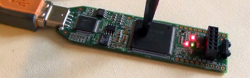
You have an FPGA circuit and you want the user to interact with your circuit by pushing a button. Clearly, you need a button, right? Not so fast! [Clifford Wolf] recently found a mysterious effect that lets him detect when someone pushes on his iCEstick board.
The video below shows the mystery circuit (which is just the stock iCEstick board), which appears to react any time you flex the PC board. The Verilog implements a simple ring oscillator (basically an inverter with its output tied to its input).
Here’s an excerpt from his Verilog code:
// ring oscillator
 wire [99:0] buffers_in, buffers_out;
 assign buffers_in = {buffers_out[98:0], chain_in};
 assign chain_out = buffers_out[99];
 assign chain_in = resetn ? !chain_out : 0;
SB_LUT4 #(
 .LUT_INIT(16'd2)
 ) buffers [99:0] (
 .O(buffers_out),
 .I0(buffers_in),
 .I1(1'b0),
 .I2(1'b0),
 .I3(1'b0)
 );
He compares the output frequency to a known frequency from the onboard crystal oscillator and registers large shifts as a push. At first we thought it might be mechanical flex on the crystal, but if you watch the video, the output of the ring oscillator is clearly shifting on a touch. Presumably (and this is a guess), small changes in the capacitance and other circuit parameters have an effect on the ring oscillator’s frequency. [Clifford] says he has many theories, but doesn’t know which one (if any) is correct.
We can’t decide if we’d depend on this effect or not in practice. But it does seem repeatable in the video. Maybe [Clifford] has invented a new product category: the Field Programmable Gate Array and Switch (FPGAS). We’ve mentioned [Clifford’s] work before on project iCEstorm and even used his open source tool chain in our FPGA tutorial (look for another one soon, by the way).
Thanks for the tip [James Bowman].


Didn’t mikeselectricstuff show this same effect on the internal RC oscillator of PIC micros a while back?
you beat me to it, whats crazy weird I was going to write a comment starting with “Didnt mike make a video ..”, so almost the same :D
https://www.youtube.com/watch?v=UCXCLR3xq8U
http://www.damninteresting.com/on-the-origin-of-circuits/ and http://hackaday.com/2012/07/09/on-not-designing-circuits-with-evolutionary-algorithms/
It’d be interesting to see if there was any mechanical stress or shock specifications for the part in question. Most things that include oscillators (at least the ones that care about accuracy or stability) do (or at least should).
re-solder the FPGA? Or the problem with the FR4 insulator layer? the noise issue or the Power/GND have not enough cap?
It’s a capacitive effect. Not a fault in the soldering or substrate. These is no need to apply force to the FPGA to see the effect.
The first thing I think when I see electronic circuits reacting to mechanical stress is that someone needs to check the solder joints!
That being said, this is pretty cool. :)
I wonder if you could make the most expensive microphone array on the planet using this technique :)
The chip is acting as a strain gauge. I have seen that happen at a previous job, where a precision analog chip was drifting depending on the pressure applied to the test socket.
yeah, it is also a thermometer. and a voltage sensor.
“We can’t decide if we’d depend on this effect or not in practice.” Unless you can compensate for the voltage and temperature sensitivity, no, you shouldn’t use it. And even then, it is useful only for a one-off experiment, as it would need to be calibrated chip by chip.
https://en.wikipedia.org/wiki/Piezoresistive_effect
Children in Africa could’ve programmed that FPGA. You monster!
Hmm… That ESD mat he’s jamming it into couldn’t possibly be related, nope.
its far more common than you might think .. built in RC oscillators in micros change frequency commonly when pressure is applied due to a similar problem
AVRs experience this /really/ clearly, too: https://www.youtube.com/watch?v=vUPaznV91PU
Chinese solder joint switches.
This is probably the article with the highest percentage of stupid comments here on HaD.
It’s pretty high, but I have seen worse.
Much worse…
But for really, REALLY stupid comments you have to visit Dave ‘the semi-hysterical aussie’ Jone’s EEVBlog.
The classic example is the Braun toothbrush teardown. The comments on that really do have to be seen to be believed.
I haven’t seen anyone mention this in the comments so far:
In process technologies starting around the 65-40nm nodes, strained silicon is actually used to improve cmos performance. This amounts to forces applied by compressive or tensile dielectrics applied around the mosfet channel. This makes these transistors especially sensitive to external forces. I made 40nm ring oscillator tester and applied small downward forces with probes and I could change their frequency and even their leakage (ioff).
Even before intentional strained silicon mosfets, it has been know that analog circuits were particularly sensitive to strain. I am aware of a case in another company where a circuit worked fine when tested at wafer probe (wafer level testing), but after packaging in an epoxy+filler package, the stress caused mismatch and caused the circuit to fail. You could even do an acid etch to partly decap the package over the circuit and it would work again.