As time marches on, so does the need to have the right tools to deal with the ever increasing popularity of SMD components. Ok. Maybe “popularity” isn’t the best word choice, as there are plenty of people out there that prefer through-hole components for ease of prototyping. But, whether you like it or not, you’ll eventually need to deal with SMDs.
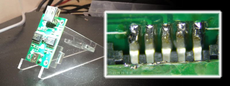
One of the problems with smaller packages is that with such small pins, their solder joints are difficult to inspect with the naked eye. A lighted magnifying lamp will only let you see so much. You can switch to a jeweler’s loupe for a quite a bit more magnification if you like – but nothing beats a microscope on your workbench. Unfortunately, unless you’re willing to spend the price of a used car on a microscope, the limited depth-of-field (DOF) can be a concern. It’s often handy to hold the PCB and move it around at different angles to get a good view of the solder pad fillets. But then you’re fighting the a very small DOF, and the steadiness of your hands.
[Tom Keddie] came up with this super simple hack – it’s nothing more then an angled PCB holder. It allows you to view your PCB at 30 or 60 degrees. Sometimes it’s the simple things in life that make your work that much more enjoyable. You can find the source files on github. And have a gander at our overview article if you’re thinking of getting your feet wet with SMDs.
[via Dangerous Prototypes]


For this I usually just use a huge(!) blob of blu-tack, but this seems much better. Will cut one the next time I pass by a lasercutter. Thanks.
But of course, the day I can afford a Mantis (and the wife allows me) this won’t be an issue. ^_^
I know. I wish Mantis scopes could be found used as often as dissection/lab microscopes are. Sigh.
It doesn’t necessarily have to be laser cut. All these straight lines and simple angles can be fabricated with a hand saw.
This is a good idea, and I might just have to come up with something similar to help me deal with my crappy $20 USB microscope.
I couldn’t be bothered trying anything that works over the limited bandwidth of USB.
I want to go from camera to screen. I can do the screen part (in FPGA) Just need to learn more about camera sensors and optics.
I found a old video camera in the junk room today. Perhaps it will be donating the optics.
I completely disagree with you. I can blow an 0603 part up to full screen at 1920 x 1080 at several frames/second. I suspect that some of this is software extrapolation, but who cares? It works for what I need, and instead of investing my valuable time into a project that would likely take a significant amount of time to construct, code, and debug; I have the exact tool I need for a mere $20.
I prefer a solution that allows you to clamp the pcb at every angle you want, and is actually heavy and sturdy enough so you can solder/rework directly under the microscope once you spot a bad solder joint. There are some nice designs for 3d printed pcb holders on thingiverse and other free 3d-model repos. Not shure if there are better solutions out there for those who have access to laser cutter but not a 3d printer.
The professional (and expensive) thing for this I’ve seen multiple times is a “grantie tilting table” ( http://www.opto.de/cms/index.php?article_id=177&clang=0 )
a vice is generally good at that. also easy to find.
My Panavise does this job quite nicely, and didn’t even cost very much.
is this really an article, Panavise is the only solution to hold a PCB that is worth mentioining.
A cheap way to get a usb microscope is to buy a mobile phone case with a microscope on it. I bought one for my galaxy s4 a few years ago , and anything SMD that needs to be looked at, I use this, coupled with an app that will display my screen’s camera on my monitor, either usb or wifi. There is noticeable lag doing this, because the display isn’t real time on the monitor. (Its real time on the phone, if you only use this screen.)
For holding the board i just use a ‘handy hands’ which is a base with crocodile clips and magnifying glass and for visuals i either use my Cell phone (Galaxy A5) or my cannon with cheap $5 macro spacer rings and a table top tripod with lift, I can view direct via usb and also take HD shots and video for display later. that does not stop me lusting after a good USB microscope, this is just my solution.