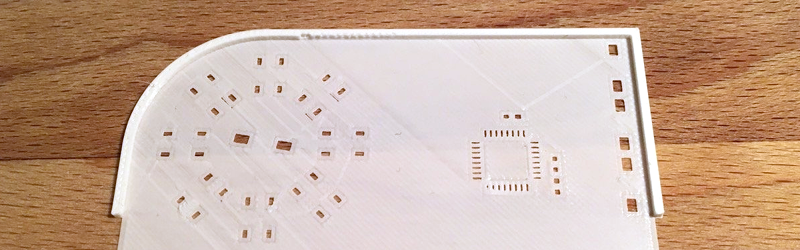
If you are soldering with paste, a stencil makes life a lot easier. Sure, you can apply paste by hand with a syringe, but a modern PCB might have hundreds or even thousands of pads. Like a lot of us, [Robert Kirberich] doesn’t like paying to have stencils made and he wondered if he could use his 3D printer to make stencils. He found the answer was yes.
[Robert] uses a hot plate to do soldering and Python to build the application to convert two Gerber files into an STL that will cause your printer to produce a workable stencil. Obviously, the thickness of the stencil has to be at least the minimum layer height of your printer. If you use Eagle, [Robert] has a script to help you, but any Gerber files of the board outline and the paste layer should work.
You can find the files on GitHub, or you can use the application on the Web. The Python code converts the Gerbers into .scad files processed by OpenSCAD. If you prefer tin cans to plastic, we’ve got you covered. You can even use beer cans if you like. If you haven’t used a solder stencil before, you might enjoy the video from SparkFun, below.


Robert! You are great! I’ve got to try this.
Interesting shelving hack in the background, turning the wire racks upside down to make a lip to limit the size of things you can shelve, and incidentally preventing stuff falling off the front. Is Boulder seismically active?
Or he has a cat.
I…always thought that was right side up. (Reading instructions and doing home improvement sober is for chumps :/)
Yep
I don’t know, laser-cut seems the simpler route.
That is, if you have a laser cutter.
Or at least access to one. For me that stencil looks very crude. I don’t think it works for 0,5mm pitch QFPs (which you still can hand-solder) or even QFN, which are awful to hand solder.
Yeah the accuracy will never be as good as a laser-cut stencil. The smallest pitch I’ve tried it with is 0.8mm, and that’s the absolute limit for my printer. If you have a smaller nozzle you can easily get down further though. For smaller pitches the whole area becomes one large hole in the stencil (which still is better than hand-syringing though).
I did a 0.5mm part yesterday, it was like my 4th smc solder ever. I realized a vacuum hot plate I bought for display panel glass separation goes up high enough to melt leaded solder paste (only use it 60-80c range for display glue). I used the hot plate to get the ground plane connector under it and bring the entire board up slowly. solders one 1-3 I had thought me that the issue with that pitch was that i kept geting too much paste on the pads. I put the thinest line I could on the back (away from center) side of pad )then half wiped it off the pads. I touched up the little tips of pads exposed using a 30x jewlers loop and my hakko station (the one that some engineer decided to delete a button from in the design phase. ive gota plan on where they will get that controller iron shoved if i come across them. ) Id say it really wasnt bad but i have nothing to compare it too lol. I finished having enjoyed it so i can say it wasnt hell but it still has that new thing smell to it…or the flux is rotting my brain idk
QFNs are monumentally easier to hand solder than QFPs. You just need hot air, paste, and a board properly made with mask between pads. Lay a bead of paste along the pins, drop the part, heat it and when the paste reflows, tap it into alignment and tap down on top to force solder out. Solder bridges between pins can be cleaned up trivially with an iron.
Way, way easier than QFPs which don’t self align easily.
In the video he says the leaded solder paste is more harmful than the lead-free. I do not agree. The flux in the lead-free is much more aggressive, and both types of solder paste require ventilation when soldering. The lead never gets airborne unless you heat it to 1749 Deg c.
I don’t use leaded solder because end users handle the circuit boards. Makes it a pretty easy decision, and processing lead-free stuff is simple once you get the process down. Agreed with your comments re:lead fumes though, that isn’t the issue for Pb stuff.
I only use lead free – better specify it – when I DON’T solder the board myself. So when I order a production run, the manufacturer has to use lead free, he has the proper equipment to do it.
For anything I do myself (lab, prototype, hobby) I use the “good old” Pb containing solder. I do not want to have the hassle of getting right the narrow process window for lead free in a – more or less converted – toaster oven.
Electronic is no candy to lick on it. And solid metallic lead is not that dangerous. There are still people getting there drink water supply at home through lead pipes.
I only use leaded solder when attaching Leds to lollipop pcbs and pacifiers. i tried it on other things but as you mentioned…it just didn’t contaminate them enough to justify the criminal charges. /s people are stupid. in maybe 3rd grade my father and I built a battery operated something (I think it was an electric magnet with lead core on a paint stir stick and all wraped in tape) that involved a piece of lead. my parents are usually a minimum of 10 years older than my piers and remembered even playing with mercury in school. well a friends mom who was not of that generation flipped shit and wouldnt let it in her house when she learned what was under the tape.
I only use lead free because eventually everything I make will end up in a landfill or recycling center. Overall it reduces the risk of environmental lead contamination. Personally never had an issue with it’s soldering ability or quality.
someone called it: http://hackaday.com/2013/06/14/machining-beer-can-solder-stencils/#comment-1015952
someone said it: http://hackaday.com/2013/06/14/machining-beer-can-solder-stencils/#comment-1015952
If only my printer was this accurate.
It seems like a step too many to me. Why not stick the solder syringe to the head mount and just use Gcode to squirt it where you want it.
I tried a similar 3D printed stencil technic for salt water metal etching.
It works quite good.
http://solder-stencil.me/: “Server Error (500)”
Darn :(
The app runs on a tiny DigitalOcean VM, it may have gotten briefly overwhelmed. Seems to work fine now, though!
Nice for a HaD article, but sadly this is far from practical.
There are too many issues with such a stencil to list here. Here’s just a few: if surface is not perfectly polished (flat) tons of paste will be wasted; the accuracy of plastic filament cannot possibly be used for anything smaller than 0603 pads with any accuracy in mind; not flexible but brittle, major issue. Thickness is also so crucial I cannot stress enough. Most production stencils are 0.1mm thick, the thickest I’ve worked with are 0.15 and they mostly felt too thick for fine pitched parts.
For DIY purposes I’ve used laser ethched mylar stencils for entire PCB panels with great success:
https://www.youtube.com/watch?v=zyB-01p7AtI
Also for the extreme DIYer here’s my soda can stencil method, with a little patience can yield stencils that outlast your PCB revisions:
https://www.youtube.com/watch?v=JWUJtmgh55M
Cheers,
Felix
LowPowerLab.com
If this stencil works it would be super convenient for prototyping!
Also, lead free solder is still bad if ingested, and it can absorb through the skin of children if you leave residue around.
I’ve done one proper run with a real board now – there are some limitations but, at least for the type of board I make, it works really nicely.
I’ve written it up here: https://hackaday.io/project/9550-solder-stencilme/log/31713-first-real-board-is-working