There are many obstacles in the way to turning carbon nanotubes into something useful. Materials engineers at the University of Wisconsin-Madison have now brought carbon nanotubes (CNTs) one step closer to becoming practically applicable for semiconductor electronics. In particular, the team managed to assemble arrays of carbon nanotube transistors that outperform their silicon-based predecessors.
One obstacle the researchers had to overcome were metallic impurities, which are present in arc-discharge-generated carbon nanotubes and practically short-circuit the materials semiconducting properties. To get rid of these impurities, the researchers developed a sorting mechanism based on a solution of polymers which wrap around the CNTs and, under special conditions, select the good, semiconducting carbon nanotubes from the bad ones with a purity of 99.98 %.

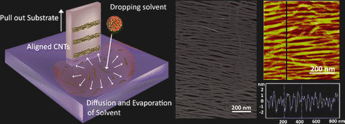
Another challenge was the alignment and spacing of the carbon nanotubes on a wafer, where the production of performant transistors requires the tubes to be aligned in parallel and with a certain pitch. The team’s scalable and fast “floating evaporative self-assembly” (FESA) process achieves this by slowly pulling a substrate vertically out of a water-bath with the previously generated solution of high-purity nanotubes floating on the surface. This causes tubes to self-align on the substrate at the air-water interface while the solvent evaporates. Baking the resulting wafers afterward removes the non-conductive polymer wrapper from the sorting step.
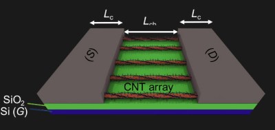
To turn the deposited carbon nanotubes into transistors, the wafers are first coated with a PMMA resist and then patterned using electron-beam lithography. The unwanted regions are then etched away before the resulting transistor structures are freed from the remaining PMMA with acetone. Finally, palladium contacts are deposited to interface with the transistors.

This new process chain results in carbon nanotube field effect transistor (FET) arrays at a density of 50 transistors per micrometer and with quasi-ballistic conduction, a fast-lane conduction state where electrons travel almost unhindered through the nanotubes, thus obeying Newton’s second law of motion. Under test, these transistors show a conductance of 1.7 mS/μm and a saturation current of 900 μA/μm, which the researchers describe as 1.9 times the current in state-of-the-art silicon transistors of the same size and architecture.
The research paper describing the process and its results marks an important milestone in carbon nanotube research. For the first time, carbon nanotube transistors are manufactured in a scalable way and with properties that can at least compete with silicon and gallium arsenide. Since carbon nanotube research breakthroughs keep happening at regular intervals, the return of tube-logic is at least foreseeable. Enjoy the video below, where the researchers explain the significance of this development.


This is quite interesting but unfortunately we have the more basic problem of being unable to mass produce carbon nanotubes of an arbitrary length. Without that particular advancement, such a device will be too expensive for anyone but groups like the DoD and the NSA. Without mass production, I’m not glad to see this kind of advancement.
“…not glad to see this kind of advancement.”
Hmph!
I’m sure eventually mass production of clean nanotubes will come to fruition…
Just extrapulate them through a decarbonizer and then resconstitute them in a spinning matrix array! My god, man, haven’t you studied a bit of science?
You could always build a Interocitor – it does everything
I’m a doctor, not a materials scientist!
DAMN IT JIM!
Next on the list “transparent aluminium”
@ FyLyX: https://en.wikipedia.org/wiki/Aluminium_oxynitride
We’ll have to settle for transparent wood for now.
That’s funny, I was thinking mass production would be useless without the purity problem solved. So glad things can be worked on in parallel.
Don’t forget that regular silicon transistors used to be in that same boat of curiosities that weren’t affordable to produce.
Now think, how many billion of those did you use to leave this comment?
ha haa!! its a modern BS170
Elektor history
So tubes were replaced by transistors and now transistors will be replaces with (nano)tubes?
Revenge of the tubes?
Carbon tube audiophile grade?
This is OK, as long as no power has to be wasted to heat a cathode.
“Get that authentic tube reverb and echo effect by sending your electrons down actual tubes. Even gold wire constrains your audio, forcing the signal to, at best, float around the outer layer of the wire. With these, you not only get the same sound effect as with silicon transistors, but you get the added benefit of your signal electrons physically bouncing around in the nano-tubes. Remember, those OTHER brands claim to use CNT transistors but we wire the whole circuit with them.
Buy now for $800,326,493.99* and here the benefits!**
*Price of amplifier circuit only. All knobs, cases, interconnects, and speakers sold separately.
**sound benefit only guaranteed if you don’t have any metalic wires or optical links in the chain from source to speakers. Even the best optical connections only allow photons to bounce and you want the sound that only electrons can give.”
Don’t break them they get angry when you poke them they start talking about headphones.
Perhaps. But (as you surely know) carbon nanotubes have nothing to do with vacuum tubes of old.
Vacuum transistors works similar to vacuum tubes by steering electrons produced by an emitter mechanism however there are significant differences, they doesn’t use a hot emitter – they use field emission, and if manufactured on a small enough process they doesn’t even need a vacuum to function.
Let’s see how far this technology will evolve. Assuming they are able to mass produce it.
i believe as time goes by, this CNT tech can evolve into processors and the like. im not sure when but i think its possible.
They have to engineer obsolescence period creating something better since when do we do this anymore.