We’re used to reflow soldering of our PCBs at the hacker level, for quite a few years people have been reflowing with toaster ovens, skillets, and similar pieces of domestic equipment and equipping them with temperature controllers and timers. We take one or two boards, screen print a layer of solder paste on the pads by using a stencil, and place our surface-mount components with a pair of tweezers before putting them in the oven. It’s a process that requires care and attention, but it’s fairly straightforward once mastered and we can create small runs of high quality boards.
But what about the same process at a professional level, what do you do when your board isn’t a matchbox-sized panel from OSH Park with less than 50 or so parts but a densely-packed multilayer board about the size of a small tablet computer and with many hundreds of parts? In theory the same process of screen print and pick and place applies, but in practice to achieve a succesful result a lot more care and planning has to go into the process.
This is being written the morning after a marathon session encompassing all of the working day and half of the night. I was hand-stuffing a row of large high-density boards with components ranging from 0402 passives to large QFPs and everything else in between. I can’t describe the board in question because it is a commercially sensitive prototype for the industrial customer of the friend I was putting in the day’s work for, but it’s worth going through the minutiae of successfully assembling a small batch of prototypes at this level. Apologies then, any pictures will be rather generic.
![Would we be insane to use a pick-and-place machine for this job, or are we insane not to have used one? Peripitus [ CC BY-SA 3.0 ], via Wikimedia Commons.](https://hackaday.com/wp-content/uploads/2016/12/892px-pick_and_place_internals_of_surface_mount_machine.jpg?w=400)
So there we were, setting out to make a batch of eight prototype PCBs. The story didn’t start on the build day, instead a few weeks ago the Bill Of Materials, or BoM, was exported from the CAD package, and the task of sourcing all the components began.
It stands to reason that the complexity of component sourcing increases with the number of individual component lines in the BoM. If your design consists entirely of generic components that every supplier has by the reel then sourcing is as simple as making the order, but sadly very few real designs are like that. So this step became an involved trawl through an array of suppliers for the elusive parts, sometimes ringing company reps to beg a few free samples.
The Great Gathering of Components
In the days running up to the build, a variety of packages arrived containing the components. There began the second major task, that of collation. It’s necessary to both ensure that everything has arrived and is the right component for the job, and to index and array them in a form such as to make the placement on the boards as easy as possible.

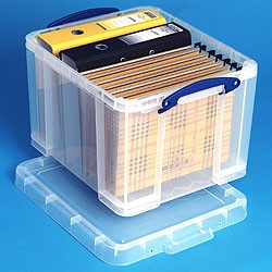
We started with a storage box of the type designed to hold hanging files. Each hanging file was labeled with a range of numbers corresponding to BoM lines, so 1 – 5, 6 -10, 11 – 15, and so on to the end of the BoM. Every line on the BoM spreadsheet was checked, that the component was present, was it compatible with the package it should be on the board, and was it present in sufficient numbers to populate the boards. Its line number from the spreadsheet was written on the label, and the spreadsheet was updated to show that it was present. The numbered bag of components was then placed in the appropriate hanging file for its line number, and the process was repeated with the next line number and so on until the whole BoM was covered.
At the end of the component collation, we had a box of hanging files containing numbered component lines, and inevitably there were a few lines which either weren’t quite right or hadn’t arrived. Some last-minute overnight ordering was in order, followed by collation steps for those parts.
It might seem like a lot of work to put in before making any boards, but this couple of days getting everything in a row will save you time when it comes to populating the boards, and will in turn result in better quality final prototypes.
On the day of the build, our components were all collated and we were handed a stack of bare PCBs from the board house. We set up adjacent workstations for the two of us, and set to work.
Become a Paste Aficionado
![Solder paste on a PCB, probably depositied by machineas it's much tidier than our stencil work. Ossewa [CC BY-SA 3.0], via Wikimedia Commons.](https://hackaday.com/wp-content/uploads/2016/12/600px-solder_paste_printed_on_a_pcb.jpg?w=400)
Screen printing solder paste is in principle quite simple. Align the stencil with the pads, and using a scraper spread a layer of solder paste over all the holes. When you lift the stencil away the board should then be left with a uniform layer of solder paste on each pad, ready to have a component placed on it.
Describing this crucial step in those terms makes screen printing solder paste sound so easy, but of course it isn’t. The paste consistency is very important for a large board in the way it isn’t for a small one. The paste you print on the pads will spread out over time, and eventually your closely spaced tiny pads will be completely obscured by an amorphous blob of paste. If you have a small board you can get away with it, but on a large board it’s important to ensure that the spread is not too quick. You’ll then have a chance to place your components and reflow the board while the printed solder is still well-defined.
![Solder paste. Just like peanut butter, except it's toxic and grey. Lady Ada AKA Limor Fried [CC BY-SA 3.0], via Wikimedia Commons.](https://hackaday.com/wp-content/uploads/2016/12/manufacturing_paste.jpg?w=400)
With the jig, stencil, scraper, and boards ready, and the correct consistency of paste to hand, there is one more step before spreading. Clean everything with IPA solvent; every single PCB, stencil, board, jig, the entire lot. It seems tedious, but it will make the difference between good and poor results. All drying paste residues, dirt, and oils can affect the quality of the job, and you need the best possible result.
After all that effort, the paste scraping itself is very quick. Make sure you have enough paste on your scraper, draw it across the stencil in one go covering all the holes with a firm pressure. Lift the stencil away, and inspect the quality of your paste printing. Don’t be afraid to clean it off and do it again if you aren’t happy with the results, we redid a couple of our board run.
Knowing Your Place
![There are 500 0402 resistors, you have to find one of them in the crowd. Where's Wally record attempt, William Murphy [CC BY-SA 2.0], via Wikimedia Commons.](https://hackaday.com/wp-content/uploads/2016/12/where_s_wally_world_record_5846729480.jpg?w=400)
Once you have started stuffing boards you are in a race against the spread of your solder paste, so there is no letting up until the task is complete. In our case the whole process took us all day and well into the evening, working through the BoM omitting any large components that would obstruct access for smaller one, then returning to fit them in a second pass. There followed a checking step during which a few inevitable omissions were rectified, no matter how hard you try there will be a few that you miss. Through all this process all that work collating components came into its own, when asked for any line I could pick it out in very short order, and I could return to it when any omissions were detected.
Bring the Heat
![Our reflow oven was a lot smaller than this one. Nelatan [CC-BY-SA-3.0], via Wikimedia Commons.](https://hackaday.com/wp-content/uploads/2016/12/640px-reflow_oven.jpg?w=400)
After a very long day and a lot of preparatory work before that, we had a row of prototype boards. We should be able to commission them all as working devices, and from those my friend will have more than enough to satisfy his customer’s demand. All of the above describes a very long and tedious process but there is no reason why any Hackaday reader should not also be able to do a large board with a bit of practice. If we’ve inspired you to have a go at reflowing your own boards of whatever size then share the results with us on hackaday.io, meanwhile if you have any tips to further streamline the process with larger boards we’re all ears.
If you enjoyed this story of a marathon small-run manufacturing session you will also enjoy [Bob Baddeley’s] series on the topic called Tools of the Trade. You should also take a look at the process used to create the Hackaday SuperConference badge.


Very nice article and description of the process. It really can be a hard financial question, but it’s very much a trade off of time vs. money. Even being in the small-volume manufacturing industry myself, I find it refreshing that the DIY tools are now good enough that this option is available for people who need to put their money elsewhere. Not that many years ago, doing this with surface mount would have been much more complex, or not possible at all. Now, as you’ve shown, you can get a great quality build on your own.
Once you have an xy file and an image of your board, creating a simple app that can step through components providing a general zoomed out view with a highlighted area and a zoomed in view showing the exact position of the next component to place is really easy. I highly recommend it if you are stuffing even a moderate number of components. Bonus points for a easy mechanism such as a foot pedal for going to the next component. Personally I usually use a small whiteboard to store components. I use double stick tape to place sections of reel onto the whiteboard and right the value or designation, components sorted in placement order (usually grouped into footprint). Be sure to tape the whiteboard down otherwise when removing tape from a reel you might pop the whiteboard up causing the tiny 0402s to jump out of the reel paper. Once you get over 2 or 3 boards, this might not scale.
I’ve done something like that for finding parts. Altium generates a pick and place file, and I have the board dimensions. That easily lets you calculate where it is, in any picture. It comes in handy sometimes.
http://i.imgur.com/8K1PSV3.png
https://gist.github.com/russdill/3081369
Dang, try a link next time…
I posted two unformatted links. For some reason hackaday decided to post the contents inline instead of just the links. Can a mod edit it?
Interesting one didn’t try a 3D printer for the solder paste (http://hackaday.com/2014/04/02/dispensing-solder-paste-with-a-3d-printer/).
Now you have two problems. :)
I have to do some big boards frequently and It helps me a lot to make several prints of the parts placement on paper and mark each of them with a different color for a specific value: one sheet has all the 0.1 uf marked, another all the 10K or 1k. etc. you see where to put the parts easily. And staring with the smallest formfactor parts helps a lot.
Oh dear. That was an exhaustive job. I am preparing documentation, stencils and so on for EMS (all electronics assembly stages) and we receive lots of prototypes. Because no one is going to order 1k of product that wasn’t tested!! We manufacture them like in few weeks (if component purchase needed), or we can put straight into assembly line in 3days. It is normal, and please let people know there is much easier way – you give Gerber’s, assembly docs, bom and in few weeks you receive product you need. Or you ship components and receive leftover components and products in a week :)
I would prefer to leave purchase stage for manufacturer, as any of them including my workplace have thousands of reels ;) so it is always ready for production and will be cheaper ;)
We work in Europe, so maybe a little trickier to work with US, but you can find local manufacturers as well. Our site is www Esemda eu
Sorry for add, but it will be easier for people to know. That there are companies which care about engineering needs and do not worry – the prices are always competitive, as there are lots and lots EMS producers around the globe ;)
Good write up. Was going to give a pass when looking at the header picture, however I spotted you saying that the pictures are replacing the confidential item.
At work, some board repairs involve re-flowing anything from >50mm^2 chips to 6-pin+soldered_heat-pad chips the size of pr58 in this article’s header picture. Hot-air rework is my choice for these things. This excludes fixing most BGA items however, Though I successfully re-flowed a few NVidia silicon die to reconnect the squashed BGA set back into conduction between the silicon and the carrier PCB without melting the BGA between the carrier and laptop main-board.
Also replaced the tiny thermal reference (offset/calibration?) resistor on an op-amp for temperature feedback to lower GPU temperatures by running the fan longer.
I managed a small assembly line for two years. The line consisted of a stencil printer, pick and place machine, reflow oven and one human.
The most time consuming task when running the line was setting up the pick and place machine. Sure, the programme could be created in as little as 30 minutes, but loading the parts onto the machine and measuring can take anywhere from a few minutes to an entire day! However, machine loaded boards are impervious to mismatched parts and tend to have greater success with QFN and BGA footprint components. In conclusion, with exception being to prototypes, I would machine load whenever possible.
“So this step [component sourcing] became an involved trawl through an array of suppliers for the elusive parts, sometimes ringing company reps to beg a few free samples.”
This anecdote is very alarming, and doesn’t speak well of the customer. If you have any control over the design phase, do the work to make sure your component supply chain is in order at that time. Don’t pick some discontinued Maxim part or min 1MM qty Broadcom part based only on the specs, then rely on the assembly house to source it from eBay. The worst case is having to respin your board, and missing all your deadlines.
My point there was that some of the parts were such fresh silicon that the only way to get hold of them was to beg some samples, the normal supply chain didn’t have them yet. To explain why would be to break NDAs, sorry, but believe me when I say there was a reason.
That makes more sense. My assumptions are showing; I guess I have supply chain management on the brain.
If you do not want to reinvent what the Chinese are already copying :-) then I think it’s normal, that you have some very new parts. So I think you gave enough explanation about the situation independent of the special product or the NDAs.
For one of the larger boards i did (manual soldering rather than reflow) I created paper templates for really common BOM items (100nF caps, 10K resistors) with cutouts in to overlay on the board then solder through.
It took a while to cut out the templates, but with a laser cutter it would be easy, and stopped silly mistakes with repeat items.