Hackaday readers (and writers) are an odd bunch. While the rest of the tech press falls over for the newest, shiniest CPU on the market, we’re the type who’s more interested the unexplored dark corners of metaphorical Silicon Alley. So when someone comes to us with a good writeup of a chip that we’d never heard about, we’re all ears.
[Remy]’s writeup of the CoolRISC 816 microcontroller CPU makes it obvious that he shares our taste for the esoteric. It has a 22-bit “RISC” instruction set. It has a dedicated 8-to-16 bit multiplier. Some of the instructions are so un-reduced that [Remy] calls bunk on its RISC claims. All of the operations, including the un-RISC ones, run in a single cycle. And the CoolRISC does this by cheating — the last stages of the pipeline run not on every clock tick, but on the rising and falling flanks of the clock respectively.
Why all these odd bits? They make the job of the assembly programmer, or compiler designer, a lot easier. With all single-cycle instructions, counting cycles is the same as counting lines of code. The not-really-RISC instructions are great for compiling C into. So what happened? [Remy] speculates that the MSP430, another not-really-RISC microcontroller that came out about the same time, ate the CoolRISC’s lunch. The MSP430 is a 16-bit machine, and chances are good that you’ve heard of TI. The same may not be true of Xemics, maker of the CoolRISC.
But still it’s nice to have someone saying the eulogy for this strange little chip. Or maybe the reports of the CR816’s death are premature — it seems to be inside TI’s bq20x80 chip that’s used in a number of battery power monitors. Oh, the irony! Indeed, watch [Charlie Miller] tear into a battery and find a CR816.
Have any of you used a CR816? What’s the strangest microcontroller architecture that you’ve ever seen?


What’s the strangest microcontroller architecture that you’ve ever seen?
Strangest? I dunno. One I miss the most? Am29CPL154.
Oh, that is a cool one (the Am29CPL154).
For me the weirdest is the NEC uPD7281 – Image Pipeline Processor. It was dataflow architecture (as opposed to von Neuman), and operating via some ‘token passing’ scheme.
archived datasheet http://www.datasheetspdf.com/PDF/UPD7281/521195/16
When was that NEC chip released? NMOS technology suggests first half of 80s.
Also, what products was it used in? It’s still quite slow to rotate images on this thing, according to the performance figures quoted. So much effort for something that still wouldn’t be real-time.
yes, that one was the first, in the early 80s, and a cmos successor the 72181 in the later 80s.
what was it used in? beats me, but I can find at least one reference to a a board for the Amiga:
https://www.researchgate.net/publication/242291029_The_ULowell_dataflow_project
I just remember having stumbled across the part in the NEC databook around 1990 and having my mind blown at such an unusual architecture. It caused me do a little research into dataflow in general, which never really caught on — possibly due to complexities in making a language/compiler for it. Anyway, I never forgot about that weird part, hence my mentioning of it here.
Pure dataflow computers aren’t popular because they are hard to scale up in hardware. Hybrid dataflow computers are common: it is called out-of-order execution.
Scaling problems are partially because operations and data are two separate entities (in practical designs) that have to be synchronized to work on a problem – and the simple way to do it severely impact performance. The main problem is that dataflow programs consists of operations that trigger when input data is available which means there have to be a mechanism to detect when to trigger all operations in a program. One could make a design where this mechanism is hierarchical, with a relatively small but fast triggers for operations that are likely to be triggered soon and in-memory triggering to detect those operations that are likely to wait a longer time.
But dataflow execution isn’t strictly deterministic and operations located close by aren’t generally likely to trigger in temporal proximity – so normal caching schemes aren’t likely to work well. The overheads to track all data flowing between operations are also a problem.
Limited dataflow execution is however standard today as noted above. Out of order execution uses parts of a traditional stored program computer and parts of a dataflow computer. It does this by using a linear fetch model where instructions being close spatially are also expected to execute relatively close temporally – so instructions are cached well. The operations for a small subset of instructions in the program are stored in a small high-speed triggering mechanism (instruction scheduler), while significantly limited to a pure dataflow design the communication overheads and the problem of fitting all operations in a program into the execution mechanism are gone.
That *is* odd. State machine, indeed.
There is no Xemics anymore, it was purchased by Semtech (maybe best know for being the company behind LoRa radios) over 11 years ago.
Semtech still uses the CoolRISC core in many of their products
I used to work for Semtech, first as an IC test engineer and later as an IC designer, and I’ve had numerous dealings with the CR816. It is a little odd in some ways (I could list a load – but I’m not permitted) and was often implemented in a somewhat non-optimal way. But, the Swiss guys liked it, knew it inside out and it worked well for us. These days it is retired, and to my knowledge nobody in their right mind would suggest using it in a new design for fear of ridicule!
So, a new Atari 2600 platform, then?
These sorts of unusual processor cores are normally only found as a sub-component of some other kind of chip application, usually due to cost and existing infrastructure. The customer never needs to know there’s even a microcontroller in there, let alone actually write their own code for it (and using a weird architecture can be an intentional choice to make it difficult for someone to even try.) Since the tasks it needs to do are fairly small, there’s almost no need to upgrade or change to another core for new and improved chips, since the improvements are usually with the application hardware and not code.
However many times an existing core is used because of development time and cost since a custom architecture is very expensive to design, much more expensive than a license for a pre-designed CPU.
My 15-year old DVD player has an ARM and an 8051 in it (Mediatek 1389 multi-core chipset), and many Nintendo consoles use custom silicon but existing cores (e.g. the 2A03 is a modified 6502, the Gameboy’s CPU is a stripped down Z80 and ARMs are used in all their newer portable systems, including the Nintendo Switch).
But in this case Semtech already had a custom core developed from the acquired company.
A very simple CPU core isn’t particularly difficult to design, and very well might have lower project risk/cost than licensing IP from someone else. It all just depends on the particular application. Integrating licensed ASIC IP is rarely as smooth as ‘drop it in and go’ – particularly once you get to even modest performance requirements (i.e. faster than a few hundred MHz). It’s also frequently encrypted, so you have limited ability to do verification/debugging, or make timing changes, and bugs are far more frequent than one would naively assume if they haven’t had the joy of integrating 3rd party IP into their chip.
Indeed. I’ve written a few cores for FPGAs. It’s possible to create something useful in a few hundred lines, with a few days work. The advantage is that you can customize everything for the application.
A bigger potential problem is software development, especially if your software is big enough that you’d want a compiler. Creating or modifying a compiler is a lot more work than creating a simple custom CPU core.
Sometimes buying silicon design from another company can bite you in the backside. That’s why Rendition failed in the GPU market. Their Verite 1000 was on-par or better than contemporary offerings from nVidia, 3Dfx and ATi, and all four were better than any other non-workstation GPU of the day.
Then Verite laid plans for their next GPU, the Verite 2000/2100. (Only a clock speed difference, only one company used the 2000 and eventually released a BIOS update to speed it up to match the 2100.) But there was a problem. A piece of chip design Rendition had bought instead of designing in-house had one tiny little bug. It took them six months to track it down, which involved tools like scanning electron microscopes to locate the flaw.
By the time the chip was ready for production, ATi and nVidia had leapfrogged ahead another generation and were alone at the table, eating all the other video chip companies lunches. They all hung on for a while, but S3, No. 9, 3Dfx, Rendition, Trident Microsostems and the rest – all defunct or bought out, merged or make chips other than ones for video.
I did send an inquiry to Micron asking if they might open source the Rendition Verite intellectual property. No reply or even an acknowledgement of the contact. :P
22-bit instructions may not be so esoteric.
PICmicro MCU, dsPIC30F and dsPIC33F devices are grouped by the size of their Instruction
Word and Data Path. The current device families are:
1. Base-Line: 12-bit Instruction Word length, 8-bit Data Path
2. Mid-Range: 14-bit Instruction Word length, 8-bit Data Path
3. High-End: 16-bit Instruction Word length, 8-bit Data Path
4. Enhanced: 16-bit Instruction Word length, 8-bit Data Path
5. dsPIC30F/33F: 24-bit Instruction Word length, 16-bit Data Path
Okay, fine, maybe a little esoteric.
8-bit PICs have a very similar architecture to many minicomputers from the 1960s and 1970s: it is in fact a simple single-address accumulator architecture. This is not surprising, because the 8-bit PIC became available in the mid-1970s from General Instruments (the company that made the AY sound chips).
Like these PICs, the old minis often had odd word lengths: the pdp-8 had a 12-bit word length, the pdp-6 had an 18-bit word length others had 24-bits or 36-bits. This was for the same reasons: computers that needed to address different amounts of RAM needed different numbers of bits for the address field.
Like these PICs, the general instruction format was: [OpCode][AddressMode][Address], where [AddressMode] usually meant either things like ‘Zero-page’ or ‘Current-page’ or would invoke an index register or cause indirection. The PIC’s primary addressing mode is ‘d’, specifying whether the result is stored in the accumulator or the target memory location.
Like many minis, when they wanted to expand the memory they used bank-switching: the 1965 pdp-8 used a 3-bit bankswitch to expand addressing from 4KWords to 32KWords and it’s proper 16-bit successor used paging to subdivide the memory space into 8 pages which could each switch in an 8Kb block on any 64byte boundary over a maximum of 4Mb. Similarly, the 8-bit PICs often have regions of addressable RAM that are banked (via the RP bits in the status or MOVLB if there’s a larger bank register) while other regions are fixed and others only semi-banked.
But basically what it means is that the 8-bit PICs are a traditional architecture from 50 years ago.
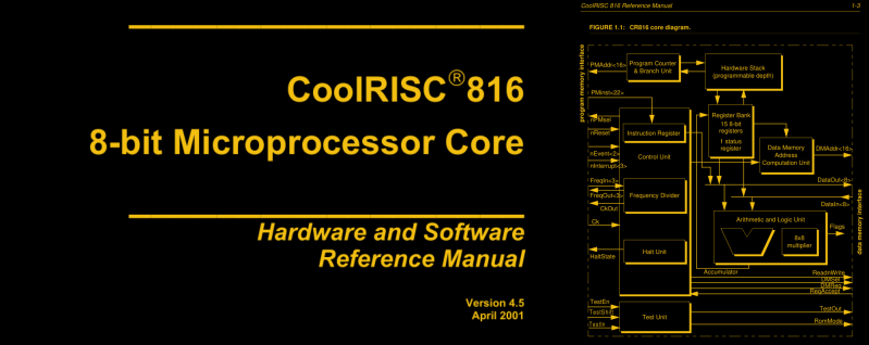
CR816 is an Harvard architecture. In Harvard architecture instructions memory beeing separate from data memory the instruction width is not constrain by data width so there is nothing odd about a 22 bits instruction width as there is nothing odd with 12, 14 or 24 bits instruction width.
Is this a joke about divisibility by 2?
I like the HP Saturn https://en.wikipedia.org/wiki/HP_Saturn
Yes, a fun one. Coincidentally I had occasion just this past week to dust off my emulator to test an HP-10C ROM image of which I recently came into possession. Turns out the trick with that image is that the LCD segment map to completely different bits in locs 09 and 0a relative to the others in the series. Who knew?
apologies, I have to amend/rescind my comment (I can’t edit/delete, so I have to follow-up, sorry); the calculator I mentioned was still on the nut processor, the predecessor to the Saturn. The Saturn was running behind schedule, and those calculators were called ‘Voyager’, allegedly because they got us on our way to the Saturn.
A very interesting architecture for sure! I type this as my trusty 48GX sits to my left.
It’s good as a first learner for assembly programmers.
As you wrote, if there is something unusual, we’re all ears. I looked at it a little bit. This CPU handles the borrow (the carry while subtract) the same way as the 6502, ie the carry is inverted, As opposite to 6809, Z80 etc.
yes and also like the ARM and others
https://en.wikipedia.org/wiki/Carry_flag
As I understand, handling carry/borrow that way leads to some transistor level efficiencies, but as I am not a silicon designer, alas, I cannot comment more on those…
“What’s the strangest microcontroller architecture that you’ve ever seen?”
The Intersil 6100. Which was a CMOS version of the strangest architecture and (required) programming tricks ever seen: the PDP-8.
Motorola MC14500 1-bit CMOS microprocessor.
I’d forgotten about the 14500; you win!