By now, most of us have had some experience getting ROMs from classic video games to run on new hardware. Whether that’s just on a personal computer with the keyboard as a controller, or if it’s a more refined RetrioPie in a custom-built cabinet, it has become relatively mainstream. What isn’t mainstream, however, is building custom hardware that can run classic video games on the original console (translated). The finished project looks amazing, but the prototype blows us away with it’s beauty and complexity.
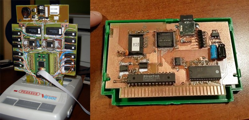
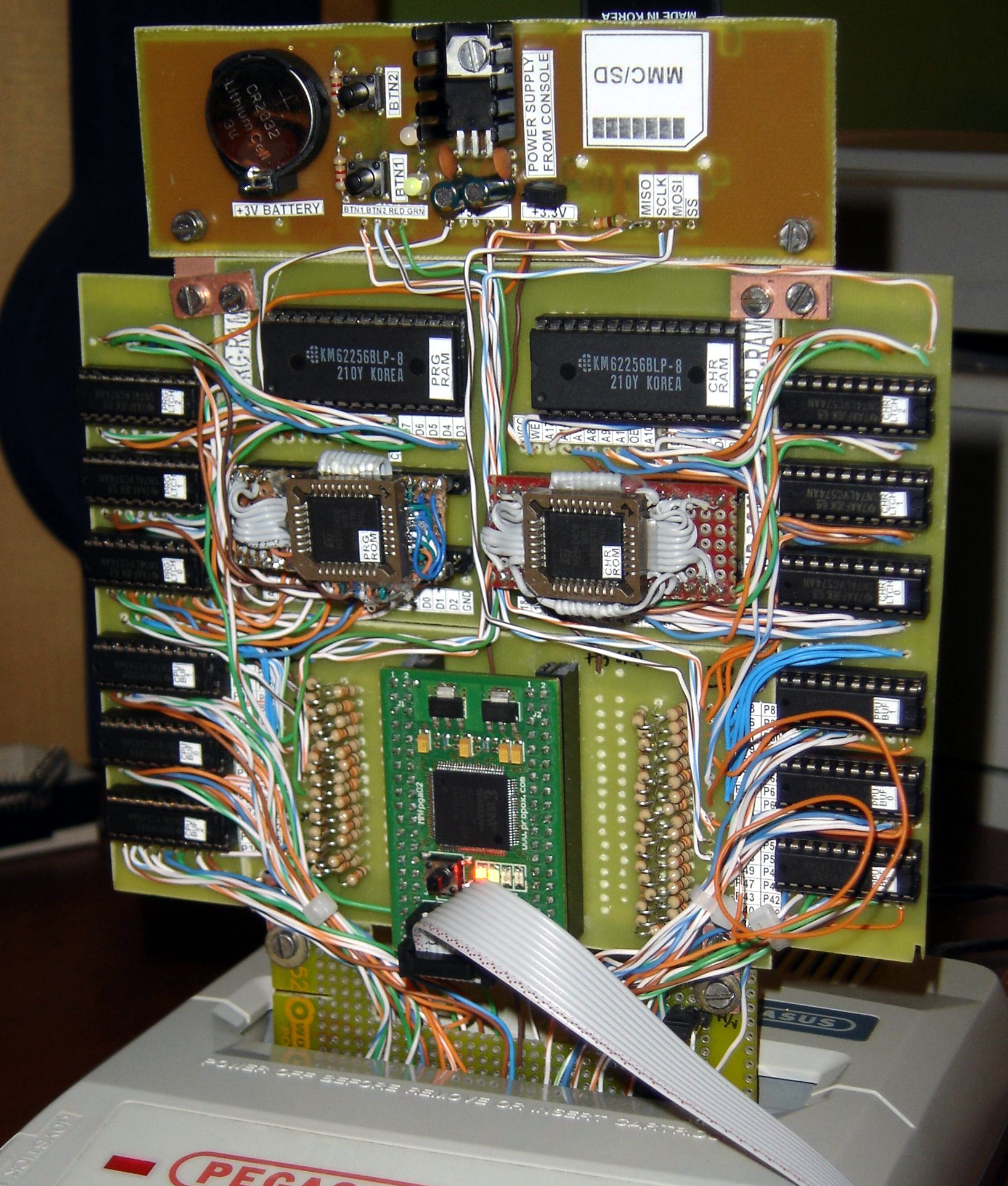 [phanick]’s project is a cartridge that is able to run games on the Polish Famicon clone called the Pegasus. The games are stored on an SD card but rather than run in an emulator, an FPGA loads the ROMs and presents the data through the normal edge-connector in the cartridge slot of the console. The game is played from the retro hardware itself. It takes a few seconds to load in each ROM, but after that the Pegasus can’t tell any difference between this and an original cartridge.
The original prototype shown here was built back in 2012. Since then it’s been through a few iterations that have reduced the size. PCBs were designed and built in-house, and the latest revision also includes a 3D-printed case that is closer to the size of the original Famicon cartridges.
Even if you don’t have an interest in classic video games or emulation, the video below is worth checking out. (Be sure to turn on the subtitles if you don’t speak Polish.) [phanick] has put in a huge amount of time getting all of the details exactly right, and the level of polish shows in the final product. In fact, we’ve featured him before for building his own Famicom clone.


Nice project but that is the ugliest soldering job I have ever seen.
You obviously haven’t seen mine
It’s not that awful for a board without soldermask…
Sorry but I have to disagree! Considering that this is a home made PCB WITHOUT a soldering mask I must say that he did a very good job. The pitch of the components pins (and therefore the spacing between the traces) is very close to what is even possible on a DIY PCB. And considering it all works this is a great example of DIY electronics and a well executed project. On a scale of 5 stars (with 5 stars is perfect) I will gladly give it the full 5 stars.
Only 5 stars! :P I gove it a solid 6 out of 5! :D
without solder mask it tends to flow and stick everywhere. I have done way worse using copper clad perfboard with traced created with an X-ACTO knife and Dremel. (sorry, I don’t have pics and I’m not going to dig through 20 year old boxes of junk for failed op-amp and JFET experiments)
The Altera EPM240T100C5N is 0.5mm pin pitch from memory. The Flash chip looks like it’s 0.4mm
The only thing I do differently is to use some Kapton tape to limit how far the *mess* can spread.
These are home made boards, probably toner transfer method. No silk screen, no overlay, no solder mask, no conformal coating and no through hole plating.
You really cant hand solder much better than this.
“(Be sure to turn on the subtitles if you don’t speak Polish.)”
“and the level of polish shows in the final product.”
pun intended? :D
“the level of polish shows in the final product”. Obviously, it’s Polish cartridge :D. It’s now a commercial product, costs about 330PLN/83USD.
Everdrive anyone?
Really hope this guy joins HaD.io could use some more powerhouse engineers/hackers like him
Isn’t this just “guy builds NES flash cart, documents extremely little, offering it for sale for an extremely high markup”? NES flash carts have been done before. I’m sure some of them were done on the equivalent of some sort of programmable hardware. It’s really kinda frustrating. At this point, *how* it was done is far more interesting than *that* it was done. It’s 30+ year old hardware, after all.
I tottaly share your view, Pat. That’s indeed the typical mentality in retro-computing circles, basically a bunch of collectors who like to call themself “legacy saviours” but rather are obsessive/compulsive buyers of glorified industrial electronics, reminding them of their childhood’s hopes : be able to afford the (once) shiny expensive novelty and to do something great from it, one day.
But decades after, they achieved the first but most of them still refuse to understand and to mess with the inner workings (even when all the knowledge is a few clicks away nowadays), they just want to get the latest and greatest upgrades for their amassed and growing treasure of patiently cleansed junk, possibly to get a sense of (cheap) materialistic achievement, and impress their little community of nostalgics. So sometimes they’re ready to pay a lot to get these upgrades, and actually miss the opportunity to simply explore and understand it all, at last… Not suprisingly, the simplest logic circuitry (that could be teached to children in a saturday workshop) is still considered black magic, and afterall , they already are “power users”, a common excuse to let the tedious and dirty work to the mechanics…
Some better informed and active people amongst them, often seeking the gratification to be the gurus and “experts” (another legacy…), drive the community interest during months of development (of what could be done in a few hours by the average chinese cloner) to finally deliver the rare, thus expensive, magic product.
Therefore this is not an excercise of knowledge sharing, these people won’t provide a real tutorial to understand how things are done, just giving vague explanations with an abuse of expandable jargon since it helps to reinforce their status of masterminds. This is not “Do It Yourself”, this is “I engineered that thing you have been waiting for”, they will be praised for it and people will be glad to finance such “active developments” and buy the resulting product to share a bit of the glory as early-adopters. They are quite happy like this, so don’t bother them with explaining or learning ! :))
Now I’m not so fond that Hackaday promotes more and more these not-so-interesting “Done It For You” projects essentially to insist on their “cool” and (nothing)”new” factors, and favors demagogy instead of pedagogy.
Not only do I disagree with everything you have said I find it hypocritical that you claim members of the retro-computer group do not do the hard work to explore the inner working of computers and then complain about some-one else’s work and the lack of documentation.
I design and build retro-computer projects in my spare time. All of my (useful) work is published right down to code, PCB layouts. I use VHDL/CPLD at least in development of many projects and of course in many cases all of this has to be coded to work with an original system. Meaning coded on the original platform in the original CPUs assembly.
Sure, there is one exception here that this designer has made this one project close source and for money but (without checking) I’ll bet he has many past contributions that were open source. The *norm* in the community is open source design with open source code. There are however exceptions.
Most of my projects are here on the IO site.
If you want to criticize someone else’s work here then the expectation is that you demonstrate that you can do better by uploading your project complete with open source hardware and code and full documentation.
It doesn’t bother me at all when someone chooses to charge for a project. I myself have paid others at times because their hard work is well worth the cost and it saves me time.
This sot of thing is much harder than people realize. It’s easy to get new hardware to work with new hardware however it can be quite difficult to get new hardware to work with old hardware.
For example, in the article graphic you see a large board with lots of small DIP chips on the left and right. All of these small DIP chips are simply level translators to get a 3.3 Volt Xilinx Spartan 3 FPGA (200 k gates) to work with an old 5 Volt system.
From there the author moved to a 5 Volt Xilinx XC9536 or XC9572 which is a very small fraction of the logic size of the FPGA chip. The XC95xx series has not been in production for some time and is a rare chip now. In any case the XC95xx simply didn’t have enough logic for the function so he moved to a Altera EMP240T100C5 which is a 5 Volt *tolerant* 3.3 Volt CPLD with more gates but it also has 0.5mm pin spacing which is harder to hand solder.
This is a fairly long chain of development which is quite common when your trying to mix two different technologies that are decades apart. The only thing I would have done differently is to use 3.6 Volt regulator to lift the CPLD Vcc to 3.6 Volts to improve the noise margins for the CPLDs LVTTL outputs to the TTL retro chips.
I have walked much the same path except that I used a 5 Volt *tolerant* 3.3 Volt XC9536(XL) instead of the 5 volt version. I have a hundred of them or so because they’re cheap. I also use the Altera EPM240/EPM570 but they are more expensive at least for the EPM570.
The other thing worth mentioning here is that he made and hand soldered the circuit boards. Anyone can send some files to a PCB house! People are quick to criticize his soldering – just try it yourself. 0.5mm and 0.4mm without a solder mask gets *messy* as others have put it. It just does!!!
“the Polish Famicon clone”
Is it really a con, when it’s a Famiclone? ;)
Couldn’t you do the same with a pic and some dual port ram?
Yesterday’s post: http://hackaday.com/2017/04/12/32-bit-processing-for-the-vectrex-arcade-system/
It uses a PIC32 and dual port RAM. Coincidence? I don’t think so.
You could, but if you do, you’d miss out on the majority of games.
Most NES cartridges have an additional mapper chip inside of them designed to increase the amount of data they can store. Many of those mapper chips have additional circuitry that give them special features (like the extra sound channels in the Japanese version of Castlevania III).
Soooo old news. Everdrive is a vintage cart with an sd card slot for all your ROMs. Been out for years.
You miss the point. It’s not that this method of running ROMs is new. It’s that it’s a single-person passion project that turned out great.
This project is the embodiment of why I read Hackaday. I would love to have the skills to pull this off and some day I might get there!
It doesn’t have to be new to be a hack it just has to be something put together to do something. Just because it’s already been done doesn’t mean it doesn’t deserve to be recognized as something cool. That prototype was quite news worthy on it’s own as it’s interesting. No issues.
I think you are missing the point, this isn’t a DIY project it is an ad for a commercial endeavor (note the lack of schematics or code, and for sale price). A hack perhaps, but as others pointed out this is really just a project intended to make a quick buck off the work of others who have already done similar projects.
Always good to see the hard, long work of project evolution. However, Powerpak was doing this circa 2007 with CPLD (I think), and selling out left and right, so it’s more “mainstream” than author implies.
So, this is just another Everdrive or clone of the other dozens of flash carts?
Reminds me of a project I did a few years ago in creating a flash cart for the GB Color. Fun stuff. You learn a ton more in creating a project like this rather then just buying something. I did the project just to gain knowledge.
https://www.youtube.com/watch?v=lI_3eTn2rMo