Have you ever wondered how you could look at a chip and map out its schematic? [Robert Baruch] wants to show you how he does it and he does in a new video (see below). The video assumes you know how to expose the die because he’s made a video about that before.
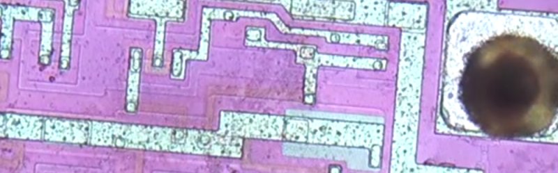
This video focuses on using his Beaglebone-driven microscope stage to get high-resolution micrographs stitched together from smaller shots. A 3D-printed sample holder keeps the part from moving around. Luckily, there’s software to stitch the images together. Once he has the die photo, he will etch away the metal to remove the passivation, the metal layer, and the silicon dioxide under the metal and takes another set of photos.
[Robert] loads the images into Inkscape so he can trace over the various components of the device and add labels. Then he uses KiCAD to produce the schematic. The end result is an entry on the Project 54/74 wiki. The project we’ve mentioned before that aims to document this historically significant family of ICs.
If you want to duplicate his efforts, be warned that you need some fairly nasty chemicals, so be careful. Real labs use hydrofluoric acid to etch glass, which is especially nasty. [Robert] uses Armour Etch, which is slower but a bit safer and easy to get and store.
A 74LS01–the subject of the video–only has 8 transistors. Imagine trying to do even a simple CPU like an 8008 with about 3,500 smaller transistors. We recommend coffee and patience.


http://www.visual6502.org/
In the summer of 2009, the Visual6502.org project shot and assembled high resolution photographs of a MOS 6502 revision D. The surface of the chip was photographed, then the metal and polysilicon layers were stripped off to reveal the conductive substrate diffusion areas. The substrate was photographed, and the substrate image was aligned to the surface image. These two aligned images were then used to create the vector polygons that form the Visual6502 chip simulation.
My microscope isn’t as good but I’ve done the same thing at home.
Lots of fun!
With hydrofluoric acid? That shit scares me.
Power steering fluid works too, only 2-3 times slower.
Raise the temperature.
You can get very dilute solutions from the hardware store, but of course it should still be treated with great respect.
I use AR grade nitric and sulfuric acid.
As Generic Human said – Should be treated with great respect.
You need nitric or sulfuric to remove the epoxy. But you need HF or fluoride to remove silicon or SiO2 layers. This can not be done with H2SO4 or HNO3.
I guess just being careful with HF is enough. It’s not like you’ll be using concentrated solutions anyway.
And Armour Etch (which isn’t a thing around here and required some googling) is basically an acidic solution of fluoride salts, so much so that the MSDS suggests treating skin exposure with calcium gluconate gel… doesn’t sound much better than other products in the market to me.
At least it isn’t instant death. With art store glass etchant, you can wear gloves and actually get some level of protection. See also: https://project5474.org/index.php?title=Procedure:Delayering
AFAIK HF is also not instant death. It is more “slow and painful death”, if you get a fatal dose.
Could you tell me what microscope and eyepiece you are using?
But it is even sold at Amazon…
I have always found HF to be too aggressive for general use when delayering/deprocessing a die. If you don’t want to work with HF; you can achieve results by polishing it with a mix of DI water and Alumina, sometimes sold as jeweler’s rouge. Don’t breathe the powder though if you can help it.
It is similar to what Chris Smith did in his The ULA Book book, with the Sinclair ZX Spectrum ULA:
http://www.zxdesign.info/book/schematicAnnotation.shtml
(Of course, since it was an Uncommitted Logic Array, it was really a repeating pattern of cells, and only the metalization layer was different, so as soon as you have one of the cells and the connections, you have the entire chip, which is easier than a fully custom chip like a microprocessor).
Very neat though I think more of this could be automated, including much of the circuit identification stuff.
Years ago I did this professionally. Might be different now but it was a very manual process then. We did work on election beam stroboscopy to be able to identify good vs bad operation but that took a huge computer back then and was never super successful.
How does he identify parts of the die?
Is there any book or article describing how this parts look like?
There are bits and pieces of this scattered all over the web, but I hope to gather all the wisdom together a little more comprehensively. Meantime, here’s a start: https://project5474.org/index.php?title=Procedure:Annotation
Al, You are the real thing! 80’s music and Inkscape!
How is this possible?
As I recall, Intel used to give away key fobs with raw CPUs embedded inside.. (Las Vegas Trade Show)
It’s possible I still have one tucked in a box somewhere.
Awesome video; it’s really fascinating to see the workflow here.
Sweet, insane amount of work and effort, kind of a fusion of art and technology, but seems to produce results!
Wow, that is totally awesome and well detailed. The only gap I have is wondering how to identify the chips individual components… though I will have to watch this more. That is really excellent what was demonstrated in the video and the video is really well made too. Thanks for sharing!
There’s a little more about that here: https://www.patreon.com/posts/reverse-workflow-16044425