I’m always on the lookout for a quality addition to my lab that would respect my strict budget. Recently, I’ve found myself pushing the Hertz barrier with every other project I do and hence desperately wanted a high bandwidth scope. Unfortunately, only recently have 70 MHz to 100 MHz become really affordable, whilst a new quad channel oscilloscope in the 500 MHz to 1 GHz range still costs a fortune to acquire. My only option was to find an absolute miracle in the form of an old high bandwidth scope.
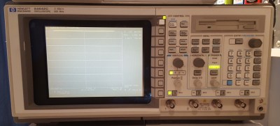
It seemed the Gods of Hand Me Down electronics were smiling upon me when I found this dumpster destined HP 54542C. It appeared to be in fairy good shape and was the Top Dog in its day. But something had to be broken right? Sure enough, the screen was clearly faulty and illegible. Want to know how I fixed it? Four letters: FPGA.
Some shallow research on this scope revealed some interesting history. This was supposedly HP’s first high end scope with an LCD and was also the precursor to the Infiniium series of scopes that would go on to rule the market. The LCD did feel like an afterthought though. The scope had an otherwise identical variant with a CRT display, and the version I acquired simply had the CRT guts removed and a colour LCD installed by HP. I hoped the LCD was at fault and not the ASIC’s driving it, this seemed like a good bet as a gentle tap would sometimes bring the screen back to life!
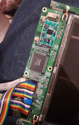
I began investigating the root cause, and started by taking apart the LCD. I found some liquid had been spilt all over it; nothing had corroded, but cleaning and reinstalling did not make any difference. Reuniting the scope with the dumpster wasn’t an option, because apart from the LCD, the scope felt like an absolute treasure trove. Even though the LCD’s driver board was completely useless now, it came from a time when the industry had not yet moved onto subatomic pin pitch on wire-to-board connectors. This meant I could conveniently solder on a standard 26 pin ribbon cable to tap off all the required signals and begin the process of reverse engineering the protocol in use.
Reverse Engineering the LCD Protocols
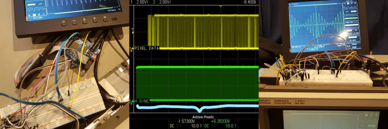
The first step of the process was to determine the signals on the connector. I was on the look-out for the most generic set of signals required to drive any LCD. This must include a few strictly periodic signals, a couple somewhat random signals and ofcourse the usual power and ground. The periodic signals would most likely be the pixel clock and the synchronisation signals which would mark the start of a new line and frame; on the other hand the random looking signals would be the actual pixel data to be displayed. Judging by its age, a fairly simple protocol was expected. Guided by this intuition I began probing the connector and soon enough I had all 25 signals figured out.
I only found two perfectly periodic signals: one, a relatively low 31.25 kHz signal gated at a suspicious 60 Hz, and the other a 25 MHz square wave. The former had to be a combined synchronisation signal. The 60 Hz was a dead giveaway as it corresponded to the nominal frame rate. The 31.25 kHz underlying signal must then correspond to the horizontal line rate within a frame. Finally, the 25 MHz signal had to be the clock for the whole system, in fact it was the pixel clock.
Next, I had to make sense of the random-looking signals which were evidently the pixel data. Firstly, the need for a 25 pin connector was clearly alluding to some kind of parallel RGB configuration. In total I found nine such signals which perfectly divides by three and concluded that the LCD was using nine bits per pixel and three bits per colour channel R,G and B respectively.
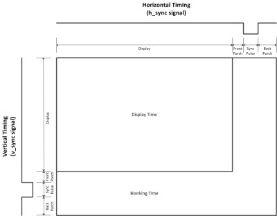
Figuring out the scheme and pin-out was part of the challenge. Perhaps more important was determining the the timings of the signals in use. Almost always, raw display signals have what are called “porches”. These can be thought of as regions within each frame where data cannot be written. These originated in the days of CRT where the physical beam of electrons took time to sweep from the end of a line back to the start of the other, or even from the bottom of the screen to the top. Although less pronounced in modern electronic screens, these regions still exist because the LCD controller takes time processing and shuffling incoming data.
Determining the timings
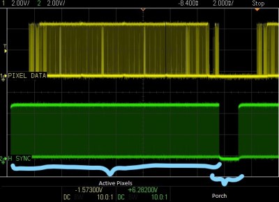
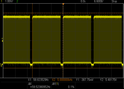
To extract the timings I tried to correlate the pixel data with the synchronisation signals. I was looking for any regions where the pixels were consistently unasserted.
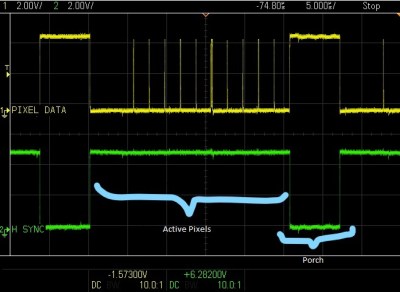
After staring at the data for a while, it was clear the LCD was using a simple, single porch scheme on both the horizontal and vertical portion of the combined sync signal. This was easy to determine because the pixels were set to either all high or all low during this period. Once I had pinpointed these regions, I used the cursors to measure their duration and translated that time to an equivalent number of pixels.
This was a critical piece of information that would ensure a stable and correct reproduction on the VGA monitor. The plan was to feed these values as constants into Verilog, and use counters to “trip” the corresponding logic to achieve the required waveforms.
Lastly, the LCDs’s resolution had to be determined as I would have to run the replacement monitor at the same settings. This was done by simply measuring the various active periods and comparing them to other signals such as the pixel clock that had a period 40 ns. The horizontal active time was measured to be around 25.7 us, hence constituting of a total of 642.5 pixels and similarly the vertical active period was 15.42 ms and with a horizontal period of 30 us, that corresponds to 481 lines. Clearly this was a standard 640 x 480 display with a refresh rate of 60 Hz.
Finding an able substitute
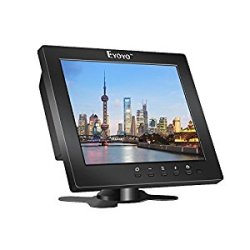
So the existing display turned out to be pretty ordinary in the end, and a replacement seemed entirely plausible. Unfortunately, the size was a bit odd; it’s easy to find seven-inch screens but eight? Even though I could not find any reasonably priced drop in replacement on the web, the size just happened to be the same as that used by many modern after market LCD installations on cars. These are nice cheap “EYOYO” branded monitors (£50) and accept literally all forms of video input from all Analog to VGA and even HDMI. They also support a much higher resolution of 1024 * 768. I’m surprised this screen is not massively popular within the Raspberry Pi community.
Finally, everything seemed to be clicking together. Not only could I replace the LCD with this VGA monitor, it would fit in perfectly as the scope even had enough room for a CRT!
So exactly, how does one perform the LCD to VGA conversion? With an FPGA of course!
Signal conversion
At this point the only thing standing between me and a functioning 500 MHz scope was successfully convert the aforementioned LCD signals to VGA. It was clear such relatively fast processing could only be done on an FPGA, but which one? My intention was to, at some point, leave the FPGA inside the scope with the screen, so I needed something small and cheap. Luckily, eBay seems to have a ton of these old Altera Cyclone II based development boards for a mind boggling £10! These are rather capable FPGA’s, hosting about 4K logic elements and ideal for a small scale project like this.
A common way these display conversions are performed are using frame buffers. The idea is to buffer a whole frame, perform the conversion and spit it out at the other end. Unfortunately this calls for a decent sized external RAM on the FPGA. These FPGA boards are notorious for not having any external RAM, hence this scheme was out of the question. After a bit of thinking, I came to the realisation that the LCD signals and VGA were not that dissimilar after all. What if I could convert from one to the other on a line-by-line basis, and circumvent the need for a frame buffer at all?
In summary:
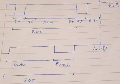
LCD has:
- A Pixel clock
- Combined synchronisation signals
- Front porch only
whereas VGA has:
- No Pixel clock
- Separate synchronisation signals
- Front and Back porch with a Synchronisation period
Going into detail of how VGA works is beyond the scope of this article, but I’ll fix that later. For now, if we simply inspect the timing sketch, we see that the only difference between the two signals is the number of occurrences and locations of the porches and the placement of valid data.
The sketch makes the conversion look simple but is only valid if the two frames are in complete sync. To tell the FPGA to start produce a corresponding LCD frame over VGA, we must first determine the start of a new frame coming from the LCD connector so that we could sync to it. This is perhaps the trickiest part of the process, because merely examining the edges of the combined synchronisation signal from the LCD is not sufficient.
We must instead measure the time between two edges and flag the occurrence of a new frame. The rest is a relatively straightforward set of logic gates that produces the above timing diagram. Lastly, as the LCD does not have a back porch or sync pulse, the incoming RGB data must be offset in time using a tiny FIFO so that it aligns up perfectly where the VGA monitor expects it. Once translating the above into Verilog was completed, I proceeded to deal with the hardware.
Hardware setup
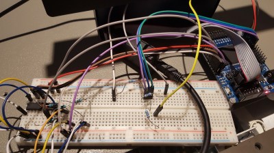
The hardware setup was luckily very minimalistic. HP was not quite utilising the LCD to its fullest potential. Inspecting the individual bits of each channel revealed a lot of redundancy: the various bits were almost always identical, indicating a very shallow utilisation of the full nine-bit colour palette. This was not shocking as HP was mostly reusing firmware from the CRT version of the scope. All of this meant that I got away with just hooking up the MSB of each colour channel with almost no loss in the final image. This saved me even more precious memory on the FPGA.
The biggest problem was that the LCD was using 5 V TTL signals. The FPGA can accept at best 3.3 V signals so level conversion had to be performed. I decided to leverage the input clamping diodes in some of the 74HC series logic buffers to perform this conversion. This tends to ruin rise/fall times significantly though. For example the 74HC4050 even has polysilicon resistors in series with the diode in the die, displacing the need for an external series resistor. I played it safe and added 1 kΩ series resistors to the input of these buffer and the output of was fed into the FPGA. The output of the FPGA’s HSYNC and VSYNC outputs were hooked up directly to the monitor whilst the RGB lines were connected via 330 Ω resistors.
Success
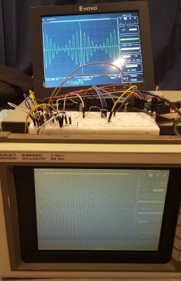
After taming the 25 MHz pixel clock to behave on a breadboard and hooking up the FPGA to the new external
monitor’s VGA port, the scope was restored to its formal glory! Although everything worked perfectly, this setup was quite noise-prone. All I need to do now is make a PCB and grant the VGA monitor a permanent residence inside the scope.
So what’s next you ask? Well, currently the only way to save screenshots is via an outdated floppy drive. But since we have now have the LCD data going through an FPGA, why not write that to an SD card?


I have been watching out for HP test equipment for some time as it was all built to incredible standards and most repair documents are available.
The downside is that people are aware of this and they command an eye-watering high pricetag even when broken.
Specifically the awesome logic analyzers. So capable… and so expensive…
I have an HP 1631D logic analyzer that I got a few years back. Judging by your name, CanuckFire, you are probably way north of me. I would totally give it to you since I have decided to upgrade… however, you would need to pick it up because I am not shipping it.
Meh. We have one of those old clunkers and work and all it does is collect dust. Nobody wants to use it. It’s big, heavy and featureless. Most of the time I’d sooner use a $5 saleae clone with pulseview. I use my beagle logic (14ch/100MHz) with pulseview most of the time. It’s a fantastic tool for the ~$15 it costed me (to get the PCBs made and the few necessary parts).
I upgraded to a legit saleae because I found a great price on it. I can save a few square feet of desk space if I get rid of the HP. I liked the HP but it’s not as intuitive, for me, to set up and run – plus the oscilloscope view is pretty slow.
those boat anchor HP 16 analyzers are THE WORSE, watching someone work on it (CuriousMarc yt channel for example) gives me physical pain. Something that is one line of python (with streaming scope) takes minutes to set up and multiple tries to capture on those 1980s museum pieces.
You only say that because you never had to deal with the alternatives that were available when the Hp came out. The HP16xx series were Cadilacs compared to the other crap of the day. Yes, you can probably get the equivalent NOW in a USB dongle. That wasn’t the case in 1982.
Great job, great writeup too.
What software did you use for FPGA, is it expensive?
Thanks! I used Altera cheap FPGA board. It goes for around £10 on ebay!(link in the article) I programmed the board in Quartus with verilog.
Your Altera II doesn’t seem to be supported by Quartus Lite – so you used a paid edition, right?
Is that expensive?
The last version of Quartus II that includes support for the Cyclone II is 13.0. You can still download the old versions from Altera’s website (the free Web Edition is enough for that device).
and NEVER install crap that comes on CDs with chinese ebay stuff. This EP2C5T144 board usually comes with cracked(and most likely troyaned) Quartus
DAMN, I have Quartus 13.1
Do you know if I can install 13.0 along side 13.1 or is it best to uninstall and then install 13.0 ???
I have been looking at these boards on Ebay but I didn’t realize they don’t work with 13.1
You can have as many versions of Quartus installed as you have disk space, they’re fully independent.
@[asdf]
Thank you for that. I just downloaded Quartus 13.0 and I was dreading loosing some of my work that is in 13.1
Nice to see software that doesn’t just completely wreck the old versions!
I had an Infinium on order for a year before they came out and I must have got one of the first.I used it for a short time and they released an update to LS120 drive from a normal floppy and then issued no updates on floppy. They wouldn’t update mine which PI**ed me off big time as I had spent £150,000 with them that year. I sold it to a Russian TV station for 3k and have never bought any HP/Agilent stuff since.
Brilliant, and the level of detail in this article is just amazing. I have a Tek scope with the same dead screen problem, but I admit I’m just not capable of pulling off a stunt like this.
Thankyou! Im glad you like it! Give it a go, the process will be more or less similar….
Which scope, and are you sure it’s a proprietary interface? I think some of the early CRT TDS scopes were EGA.
I checked, it is TDS2002 with LCD screen. Do you have any info on LCD interface, or possible replacements?
I have a TDS1002. The protocol is really simple, but the color model’s refresh rate isn’t compatible with a normal SVGA output (11.4kHz hsync/43hz vsync) so you’ll have to use an FPGA with enough RAM for a framebuffer and replay the content asynchronously with input.
Look for the service manual (“tek_tds_1000_2000_series_svc” p6-37)—it’ll give you enough information to get started. The connectors between the logic board and the LCD are “Picoblade”
Thanks, I’ll look into it. It is basically a brick currently, so I will try.
Oh. Right. And the other major difference, which is only implied in the service manual: the only difference between the TDS1002 and TDS2002 is the LCD, and whether the cable that connects the logic board to the LCD intentionally shorts out two pins is present or not. So you should be able to get 320×240@1bpp@70Hz by changing that, instead of the color LCD’s 320×240@3bpp@43Hz.
Nice hack, but I do wonder – wouldn’t have been easier to find a regular parallel interfaced LCD screen and skip the entire VGA conversion? The image quality would likely be better too.
Or, if you are putting an FPGA there, just drive the LCD panel from the monitor using LVDS – quite common for driving these small LCD panels.
The existing panel is broken, that is the whole point. Also as i mentioned, i couldnt find a replacement screen as this scope is 20ish years old. Lastly, driving the new screen using LVDS would be silly. Why risk taking apart the new monitor and reverse engineer its signals when i can just drive it with VGA?
would the fpga you used be enough muscle to convert lvds to hdmi or even vga out at 1080p?
LVDS and HDMI are not a lot different.
If the input pixel clock is the same as the output clock then you don’t need to buffer a whole frame of the color information and therefor don’t need a RAM buffer so a small FPGA or even a CPLD would be fine.
If the pixel clock is different but the horizontal line rate is the same then you need a decent FPGA with enough distributed RAM or BRAM built in to buffer one line only.
If the frame rate or mode (1080i or 1080p) is different then you need to buffer a whole frame so you would need to have an external RAM chip.
Using the term “pixel clock” here is not the most accurate because you could convert 320pixels@25MHz to 640pixels@50MHz.
Yeah, but then he wouldn’t have gotten to build an LCD-to-VGA adapter. :)
AWE-SOME!
regarding the floppy drive: There are devices that have the same form factor as a floppy drive, but save data onto a USB flash drive. They are meant to replace the drive in old IBM compatible computers. Maybe you can get one of them to work inside the scope.
Yes search for “floppy disk drive to usb emulator” (http://s.click.aliexpress.com/e/uNBq3VR) a lot of (not to old!) CNC machines use floppy disk for program loading. I upgraded some with this device
Yet another spam link (affiliate) from you.
I wouldn’t consider a relevant link as spam. Besides, they are entertaining.
https://twitter.com/absolutelyautom/status/763459385083457537
*keeps forgetting which sites auto-embed*
relevant maybe (didn’t click) but still affiliate ->spam
https://www.youtube.com/watch?v=c3zLTpDbyDc
Adil, great repair job. Congratulations on your trophy scope! :)
As Dan mentioned above, there are drop-in USB port replacements for floppy disk drives. A quick search of Amazon shows that folks are happy with $30 models.
Examples:
* Yosoo Sfr1m44-u100k Updated Version USB Floppy Drive Emulator – $32
* Generic SFR1M44-U USB Floppy Drive Emulator for Industrial Control Equipment – $20
I’m not affiliated with these sellers, nor am I getting any kickbacks. I’m just a maker that appreciates this sort of work.
These floppy emulators aren’t quite “drop in” replacements, that is why there are several versions of them.
There were two data densities: double density 720kB (DD) and high density 1.44MB (HD) and some of the really old drives will be 720kB. On some FDD emulators this can be selected with a jumper but most are 1.44MB only.
The other common variation was the use of one signal in the bus cable. This signal was originally used to indicate the FDD was READY and this is most common on 720kB FDDs. Later that same signal wire was used to indicate if the floppy disk has changed since the last read. This signal is almost always selectable with a jumper.
Hi RÖB, I know it will be off topic but I would really like to know more about floppy to USB emulators. I have an HP8713 Network analyzer that could really do with a USB port in place of its 1.44MB drive. And it need not support HP’s LIF format.
From memory (Wikipedia might give a more accurate re-collection)
Historical disk layouts that I can remember –
All the old formats were 512 Bytes per sector. Earlier system used the FDC765 controller that needed a companion chip to extract the data from the raw MFM. Later systems used a 3765 that supported higher densities as a standalone chip.
Example: 360kB = 40 cylinders * 2 heads * 9 sectors * 512 Bytes per sector
kB / Cylinders / Heads / Sectors / Controller type / Hardware designation / usage
180kB, 40 cylinders, 1 head, 8 sectors, FDC765, both 5.25″DD and 3.0″DD, examples Amstrad Sinclair
320kB, 40 cylinders, 2 heads, 8 sectors, FDC765, 5.35″ Double Density (DD), very early IBM format
360kB, 40 cylinders, 2 heads, 9 sectors, FDC765, 5.25″ Double Density (DD), IBM XT
720kB, 40 cylinders, 2 heads, 18 sectors, FDC765, 3.5″ Double Density (DD), IBM XT
1.2kB, 80 cylinders, 2 heads, 15 sectors, 3765, 5.25″ High Density (HD), IBM AT
1.44kB, 80 cylinders, 2 heads, 18 sectors, 3765, 3.5″ High Density (HD), IBM AT (HP’s DOS format)
So you are looking for a generic DOS 1.44MB 3.5″ HD emulator and there are many of these.
Most of the generic 1.44MB function the same way in that they use proprietary Floppy Disk Image File format. You can just drag and drop things like text files to the USB because the compatibility of the emulator is at a Cylinders/Heads/Sectors level and NOT at a FAT16 or FAT32 level.
This means you have to use your PC to add files to image files and then select that image file on the emulator.
Most of the emulators I have seen for 3.5HD are based on a STM32. It would be nice to add a ESP8266 to this and be able to upload/download files to the emulators via a HTTP web server. Some versions of the ESP8266 breakouts probably have enough IO to go it alone but might not have the MIPS (I would use LUA) for MFM emulation but the ESP32 can probably do the MFM emulation easily. Perhaps a cheaper ESP8266 and a CPLD for the MFM Modem and extra IO.
Also you will have to set the “Disk Change / Ready” jumper.
Correction: You can’t just drag and drop things like text files to the USB because …
Nice write-up. Do you plan on releasing the verilog?
I’d like to second that.
My 54542C has the same issue, unsurprisingly, and it would be great if I could replicate the amazing hack you’ve done.
I am also happy to help with the layout of a PCB in case you haven’t come around to do that yet.
So, can you please share your Verilog design and schematics? Maybe on Github?
Thanks!
Instead of shifting the pixels with a FIFO, you could simply shift the sync pulses instead (a synch regeneration circuit, similar to that commonly used to defeat Macrovision on VHS tapes).
I am guessing that is exactly what he did.
Those 54542 scopes are really nice! I have one of the 54542A (CRT, monochrome) that is my main lab scope. Something to be aware of, is that there is a lithium battery on the logic board that maintains all of the calibration information. Eventually, it will die. Before it dies, make a copy of the calibration information to a floppy disk, and then recovering from the battery loss is just replacing the battery and restoring the cal data from the floppy. There is an entry in the utility menu tree to do this (both directions). Calibrating one of these scopes without a full cal lab is possible, but not great.
By the way, when the battery dies, the scope will completely forget that it is a scope. The display will not show any activity, except when you push the little reset button on the back of the cabinet, you get a brief message about the battery and then goes blank.
Nice hack, enjoy the scope!
BobH
The scary thing is, something like a Cortex-M4 would almost certainly be fast enough to accomplish the same task. Might be hard to get a clean, jitter-free output. But it would be fun to try. DMA perhaps.
The Cortex-M cores have features for enabling fully deterministic timing at the expense of performance, eg. disabling tail-chaining interrupts. Also any flash prefetch/caching mechanisms have to be disabled. DMA may be easier, depending on the features of the peripheral. You probably also have to configure bus priorities so the core doesn’t stall the peripherals.
Since most MCUs have enough space, you could for example store a full line of HSYNC, using the pixel clock as trigger.
Any chance that 25 pin cable is a VESA Feature Connector?
The dumpster gods are amazing! I’ve been looking for a cheap used Workmate for at least a month and yesterday I found one in a dumpster, in pretty good condition and fully functional. People is weird.
First:
SHAKES FIST AT SCREEN SO HARD I’D HOPE IT PUNCHES THROUGH THE INTERNETS AND THROUGH YOUR SCREEN SO I CAN GRAB THAT ‘SCOPE!!!!! #Jealousy
Just kidding… Wow, you lucked out on such a dumpster dive.
Second:
There are chips that’ll convert that 21-bit parallel screen feed into LVDS (Panel-link).
The catch is trying to find a forgiving laptop screen that can be under-driven.
Under-driving some LVDS (Panel-link) displays, say 300×200 on a 1960×1200 would give a small square of 300×200 dead center of view, whereas the non-forgiving LVDS screens will either display blank, flicker, print garbage or smoke (Last one is very rare, only happened once on a whole batch of same model!)
Also those 21-bit to LVDS… some of those can operate at around 0hz and make good 16-bit per chip-pair combiners and expanders.
Then there are TMDS (DVI, HDMI, Blah, ETC) to 21-bit (or 32-bit with Least Significant Bits disconnected)
Another tip…
For black and white: Use TTL buffers in uni-direction towards the LCD and tie the red bits to the green and blue bits, i.e. R0,G0,B0 on one wire, same with RGB1, RGB2 etc. Keep each bit-set separate, i.e. don’t tie all together.
Enjoy monochrome :)
Source of my knowledge:
I work on E-POS at work… The SNIkey TFTs in use by one customer have internally:
TMDS to 32-bit converter wired in 21-bit format to a buffer set then wired to a parallel-to-LVDS Panel-link chip.
The older screens sent 21-bit at around 1.5-metres via a larger than SCSI-like cable (Yes the displays were normally off colour and dull)
Awesome job saving an awesome scope! I hate it when good test equipment ends up as landfill, which happens way too often. Glad you’ll be getting good use out of that one.
This is a fantastic write-up. Thanks for contributing it to this site. The detective skills are what makes it shine.
Great project and great write up as well !!!
I am guessing that the dot clock is actually 25.175kHz rather than 25 MHz as that is the standard for 640/480/60Hz VGA.
With three 3-bit R/2R DACs you could also have a VGA out for a monitor. You just need to separate H and V Sync as VGA LCD monitors can’t use composite Sync.
To capture periodic signals like Sync I open a window to detect the transition between 90% and 110% of the period from the last detected transition. This highly improves noise immunity.
Also a minor historical point –
Quote: “These originated in the days of CRT where the physical beam of electrons took time to sweep from the end of a line back to the start of the other, or even from the bottom of the screen to the top”
There are two older technologies of CRT.
1) The old TVs used electromagnet deflection. The limiting factor was the inductance of the deflection coils and the porches were the solution to this problem.
2) The other case was the old Cathode Ray Tube (CRT) Oscilloscope (CRO), and these used electrostatic deflection as it was much faster.
This is a spectacular, admirable hack. I will note that your efforts to get a screenshot out of it might be more easily accomplished by a gpib-to-usb converter and an hpgl-to-other-formats conversion program. Every 54542 I’ve seen has had gpib on it. But with that said, I love what you’ve done.
“These are nice cheap “EYOYO” branded monitors (£50) and accept literally all forms of video input from all Analog to VGA and even HDMI. They also support a much higher resolution of 1024 * 768. I’m surprised this screen is not massively popular within the Raspberry Pi community.” – Where did you find these for that price?
Amazon. I got it for £50
Just WHO would dumpster a $19k scope, bad display or not? Looking at what documentation I can find, the CRT model used a fairly conventional analog monitor. But the display signal was mainly generated by main CPU, so undoubtedly a firmware change…. but perhaps a firmware rollback would have accomodated use of another analog monitor. (Would be suprised if there wasn’t a VGA output on the back.)
There wasnt. Hence the effort. I suspect a firmware and hardware change because the LCD is full colour.
Makes sense. In truth I was very suprised by just how little information was available for it, even directly from Keysight. Sure not like the comprehensive manuals I was used to seeing from HP.
You can purchase 3.5″ floppy emulators with USB socket and format the card with virtual disks. The devices support selecting other disks. It’s a bit crude, but you’d then have access to the data as saved by the scope, rather than just screenshots.
+1 for “subatomic pin pitch”!