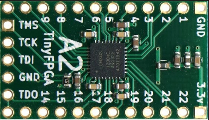
We recently noticed an open source design for TinyFPGA A-Series boards from [Luke Valenty]. The tiny boards measure 18 mm by 30.5 mm and are breadboard friendly. You can choose a board that holds a Lattice Mach XO2-256 or an XO2-1200, if you need the additional capacity.
The boards have the JTAG interface on the side pins and also on a top header that would be handy to plug in a JTAG dongle for programming. The tiny chips are much easier to work with when they are entombed in a breakout board like this. Bigger boards with LEDs and other I/O devices are good for learning, but they aren’t always good for integrating into a larger project. The TinyFPGA boards would easily work in a device you were prototyping or doing a small production run.
The files are on GitHub. According to the project’s main web site, this is the “A-series” because there are “B-series” boards forthcoming that use USB instead of JTAG, and will use the Lattice ICE FPGA devices.
The components on the board are 0603 and QFN32 packages. [Luke] suggests a solder stencil, paste, and an oven, but these size components are hand solderable, with practice.
If you want to look at the how and why of FPGAs, we covered another Lattice part in great detail, winding up with a PWM output device. Although the parts are subtly different, the work flow and principles will be the same. You’d just need the right JTAG dongle to do the programming.


The lines are starting to blur a lot between FPGAs and CPLDs as far as architecture goes
But looks like the XO2-256 does not have internal configuration flash so really the XO2-1200 is your only option unless I’m reading this wrong
Looks to me like the whole X02 is internal config FLASH –
http://www.latticesemi.com/Products/FPGAandCPLD/MachXO2.aspx
What’s LUTs in Altera or Xilinx speak? It looks like the smaller 256 LUT is about the size of a larger CPLD.
> What’s LUTs in Altera or Xilinx speak?
I’m not sure I’ve understood your question correctly, but LUT is “look-up table”. They used to be 4 input, 1 output, but it varies by chip.
The 256 does have internal self-booting config flash. It does not have any EBRs.
Atleast the Altera MAX II “CPLD” is a “FPGA”. To anyone who hadn’t seen the marketing.
Is there a 5v tolerant alternative? I’m looking for a small packages like qfn32 or qfn48.
I know you can use Xilinx XC95XL but those are clunky and using TXB0108 don’t work with opendrain busses..
Using TXS0108E would work with open-drain (as well as push/pull) busses
Have a look at the datasheets for Altera EPM240 or EPM570. Also, quite often the solution may be a level translator.
You said these components are hand solderable with practice, do you have any tips on how to solder a QFN package without hot air??
Either don’t solder the carrier pad… unless it is the only GND…
or
Have a via pad or two in order to solder the pad from the other-side of the board.
You can bake it in a pan or skillet too. A bit crude but does work for small boards and one-offs.
If you don’t want to invest in hotair or oven (should be way less then 100 USD) design the footprint with one or more via’s in the exposed pad. Make sure there is no soldermask on the other side. In eagle place a regular pad on the smd pad and ignore the drc warnings. for the other pads make them stick out longer so you can use your soldering iron for soldering those.
IMHO get a cheap hotair station as that is much faster and less errorprone..
I used a frying pan once, worked well.
I also did the frying pan method having never done SMD soldering before. I bought some paste in a syringe, and some additional tips. It was nice and easy. A little freaky the first time, but a cheap infrared thermometer helped me keep calm and know that it’s still okay.
Once I did that a few times, I spent the $50 on a hot air station to make rework easier. I LOVE using hot air to solder stuff w/ paste. Like buying a good temp controlled soldering iron, I’m kicking myself for avoiding it for so long.
My biggest concern on solder paste was worrying about the expiration date. Don’t. Just keep it in the fridge, and everything will be fine for one-off small jobs.
If the paste dries out add some acetone and/or alcohol to it and stir it again. Should be ok for hobby use..
For my first successful prototypes I used a cheap electric griddle along with some low-temp lead-free chipquik solder paste. I even managed to reflow a whole panel of 25 prototype boards this way. I just kept a close eye on the solder paste and adjusted the temperature manually.
I have since built a reflow oven using the ControLeo2 kit which is fantastic. I have successfully reflowed several TinyFPGA B2 prototype boards in that reflow oven. I wouldn’t trust an electric griddle with the 0.4mm pitch of the BGA package.
Clean surfaces and good flux will do it.
I think I was able to successfully solder one QFN32 package… along with several messy attempts XD I believe the large center pad is mostly for heat transfer out of the chip into the large ground plane of the PCB. It is not required for it to be connected but it is helpful if it is.
There are two methods that I know of to solder it by hand. The first method is to use an iron with a very fine tip (or a chisel tip) along with some fine solder. You would tin one pad to start, place the package on the footprint and then heat the one tinned pad until it reflows and the chip settles. Then solder each pad individually by first heating the pad and edge of the pin then applying solder to the joint with the iron moved out of the way but still contacting the pad.
The next method is the drag method which I attempted but failed at. It is best attempted with a reservoir tip that can hold molten solder like a fountain pen. This method requires liberal amounts of flux as the solder will lose all of it in the reservoir. You hold the chip down on the board in place and drag the reservoir tip along the edges of the package. This works very well for packages with protruding pins but is tricky with QFN packages. There is very little pin surface area on the sides of QFN packages and it can be difficult to make contact with the pins with the molten solder.
Anyways…you may not want to take my advice for hand-soldering QFN packages because I had a really hard time with it and was more than happy to move to solder paste, stencils, and reflow. ;)
I have few projects which would benefit from really fast signal processing – FPGA would be a saver for them. However, is there a decently powerful FPGA that could be used as simply as MCU on my boards? I.e. only one power rail, embedded configration memory, and preferably in a small package (less than 64 IO for example)?
Xilinx has a few devices with internal flash and small package. Minimum number of supply rails is two I think . 1.2v core and then io supply. If you need less logic: lattice. They have one rail devices.
Could you give me a tip for a concrete series of chips? I got a little bit lost in their offer.
Once things get a little more settled on A and B-Series hardware production side I am planning on porting some existing opensource micro-controller cores to these boards. The A2, B1, and B2 boards should all be capable of fitting micro-controllers and peripherals of various sizes. These boards all require only one power input and all of their IO is configured for 3.3 volts IO.
An XO2 isn’t a traditional CPLD. Lattice calls the C – ‘Crossover’. It has a more traditional FPGA logic cells fabric with two 4-input LUTs and 2 reconfigurable flip-flops per slice. It’s not a full FPGA in my book as it does not have any DSP/MAC slices. The smallest part (256 LUT) does not have any EBRs or PLLs.
It does have a self-loading internal flash (to SRAM based control) and supports programming over I2C and SPI even blank from the factory. The family also has two hard I2C M/S cores and a hard timer to save on fabric resources; each with an internal Wishbone interface that also provides dynamic access to PLL controls and user flash. XO2s are not 5V tolerant unless you count PCI clamps on one side which require current limiting. There is also built-in 7:1 input/output gearing on dedicated sides for OpenLDI/LVDS applications which can be useful beyond video applications.
I think they are nicer parts than the Silicon Blue families (iCE). Just they don’t have an open reverse engineered synthesis chain. I really wish they would make a 48 or 64 pin QFP packaging option.
the first fpga’s didn’t have DSP or MAC slices either…
Beware the hard i2c cores, the primary one in particular has some bugs having to do with its being used as an optional method for programming the flash.
I’m going to get crucified for this question, but I’ve never quite understood the advantages of an FPGA over a microcontroller, and it seems like the two are getting more similar every year. I have assumed that it can be made to run much faster and there are potentially more I/O pins. What’s the real deal?
High speed circuity on a chip that can be restructured as desired. No need to wait for the processor to finish a task, or deal with interrupts. Though you can of course add a uC to the schematic
Not crucified.. the easiest explanation is a FPGA contains the raw materials from which a MCU is made in large quantities. Every digital system, whether an ATtiny or the latest i7 is made from combinatorial logic (‘gates’ – AND, OR, XOR, etc), state elements (flip-flops), and electrical connections (wires, traces, etc). A processor is an example of a finite state machine where the current state is circulated through a combinatorial path and re-latched as the next state. New instructions fetched from memory keep altering the current state until the machine does what the user wants.
FPGAs contain these basic building blocks allowing you to create any digital circuit electronically by turning on and off junctions that connect the combinatorial elements – Look-Up Tables (LUTs) which are small ROMs contain a truth table – to state elements like D-flip-flops to create FSMs, complex FSMs like MCUs and MPUs, or specialized circuits that can be duplicated many many times within the same device for parallel speed.
Some types of problems are good for parallelization, and others are not.
Video stream decoders and DSP are some examples where the time-sensitive observer can witness the advantage. Many try to use a GPU in the same fashion, but even they are not always the right solution given the architecture is static.
Modern SoC will combine many of these operations as efficient ASIC blocks, and some FPGA will have an energy efficient ARM CPU on th die… rather than inefficiently emulating one.
For most tasks, the FPGA will be less energy efficient, but there are some types of problems that separate extremely well.
In many specialized cases, you can achieve power savings over MCUs or discrete DSPs. In one project I’m working on, the FPGA implements an image processing algorithm for a fraction of the power draw that a conventional CPU or TI DSP could achieve. (It’s a battery-operated handheld device, so low power is a critical requirement.) In this case, there are no external memories required, which saves power and board space. The drawback to this is higher cost (good FPGAs aren’t cheap) and longer development cycles (your DSP routines have to be custom-designed and -implemented in a hardware description language). I should mention the performance is very high, too. It runs a TFT GUI at 30 FPS with a lot of room to spare.
This is a common question and exacerbated by the fact that many examples you see on the Internet would be better solved by a microcontroller.
Do you remember the kits you could get from Radio Shack that had a bunch of electronic parts and some solderless spring clips? You wire up these terminals and you get a radio. Wire up these terminals and get an alarm system. These give you a metal detector.
That’s an FPGA. It is basically some logic gates that you can “wire up” to do different things. Of course, one thing you can wire up is a CPU at which point they are practically the same thing, but that’s not always the case.
Consider this. Suppose we have a nuclear reactor and we want to measure some temperatures. If the rate of change of the temperature is more than a certain amount, we want to cut power to the control rod holders so the rods drop and stop the nuclear reaction. This is very important.
With a microcontroller I could write something like:
Loop: read temp1
if temp1>threshold then power_off
read temp2
if temp2>threshold then power_off
….
goto Loop
Yeah, I could use a for loop and index, but the point is that the CPU will look at temp1 and then later look at temp2 and much later look at temp10 and finally go back to temp1. No matter how you slice it, you can only look at so many at a time and then you will not look at them later. Sure, you could throw hardware at it and do, say, an interrupt, but there is still a fixed amount of time while the processor does it stuff and it is a fraction of the CPU’s cycle speed.
However, with an FPGA I can build a logic gate that reads the temp, compares it, and drives an OR gate. The delay will be very small (logic propagation delay measured in picoseconds). And if I make 20 copies of that set of gates and expand the OR gate, the time it takes to process will remain essentially the same. If I make 100 copies, still the same.
There are more complications when you deal with sequential logic (e.g., flip flops, registers) and then clock speed comes into play, but still not in the same way as a CPU clock speed.
What this means is the jobs where FPGAs excel are where you need lots of things happening at once. Sometimes those things are related (like parallel processing of audio or video). Sometimes they are not.
If you search Hackaday for FPGA, you’ll see we’ve covered this a few times and even had some cheap starter projects.
Now all we need is the analog version of an FPGA and your analogy would be even closer. ;-)
Many companies make mixed domain products that do just that. PSoC devices from Cypress integrate simple programmable digital blocks with analog comparitors and even op-amps + a general purpose MCU. SIlego makes a line of small cheap integrated power controllers with LUTs and analog in/outs. Even Lattice makes a companion device called a L-ASC10 that adds mixed domain analog to MachXO2 devices.
A microcontroller is a discrete-time device. An fpga is like a logic circuit, doesn’t have to be clocked.
Not really true. Yes you can have a combination logic circuit only in a programmable device but it a) isn’t very useful and b) still has a discrete-time propagation delay that defines ‘speed’. As soon as you add the first flip-flop, you are in a clock domain (async set/reset aside).
You can run a FPGA at high speeds like 200-300Mhz. So you can code in the same MCU and have it run much faster than the original.
You can also have lots of parallel processes.
Also, if you do not need the small size of this board, you can get a larger XO2 breakout board from Lattice relatively cheap (eg):
https://www.digikey.com/product-detail/en/lattice-semiconductor-corporation/LCMXO2-7000HE-B-EVN/220-2625-ND/3906092
At $30, it’s about double the cost of the same single unit 7K-LUT device mounted on the board and includes USB JTAG and serial port.
Quantity Available: 0
Lead time: Ships on 9/8/17
:(
I really love Lattice’s “breakout board” line of dev boards. They keep it minimal and affordable, breakout nearly everything, let you add jumpers for all the individual power rails, and just use a straight FTDI chip as a programmer (meaning Lattice’s official tools always have built-in support for driving a generic FTDI-based programmer).
You can get Chinese FPGA boards on ebay at a fraction of the cost, and already assembled. Assembly is the problem for me-my eyes are not what they were when I was 20.
Any Opensource Board for XO2 TQFP-100 or TQFP-144 ……?