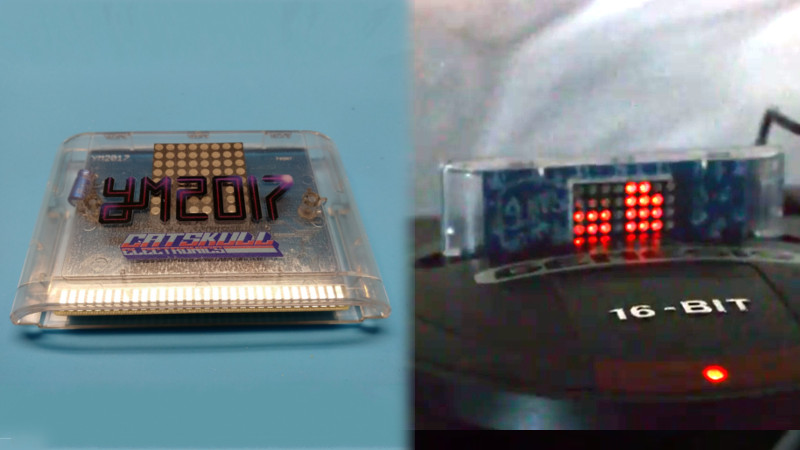
The Sega Genesis, or Mega Drive if you’re not from North America, isn’t exactly this summer’s hottest new console, but it still has a huge following 29 years after launch. Fans range from retro Sonic enthusiasts to hardcore chiptune composers, and this year, Catskull Electronics is releasing a Genesis compilation album on a cartridge with a rather special feature.
The cartridge sports an 8×8 LED matrix, which acts as a visualiser for the audio coming out of the console. They’re controlled with a combination of data and address lines with some buffers and 74-series glue logic to make it all work together. Special attention was paid to make sure the LED matrix doesn’t just respond to all activity on the bus, though it would perhaps be cool to see some blinkenlights on a 90s console one day.
Each row of LEDs is attached to an address line, and each column to a data line. It’s a fairly basic multiplexing setup which sees each LED only actually lit for a fraction of a second, but sweeping the display at speed creates a lasting display. The image data is stored as an 8×8 sprite in the system RAM, and updated with the sound level of each channel from the Genesis’s audio subsystem.
The team are looking to release the ROM code in future to inspire copycat designs, which has the potential to spawn even more Genesis cart releases in future. We look forward to seeing what else the community comes up with. And if you’re a die-hard Genesis fan, there are other ways to listen to those classic tunes too.


How about adding some temperature sensors at the bottom of the PCB, near the stripes. That way it could be programmed to blink it’s lights when you blow on it!
One of my favorite weird things about the Genesis cart is the /TIME pin. It’s asserted when the CPU is accessing the 128 word memory region starting at 0xA13000. Given the name, it was clearly intended for an RTC, but I don’t know if any games use it that way. Several pirate multicarts use it as the game selector.
Since the region is only 128 words wide, using 0xA13000 instead of 0x200000 wouldn’t make the hardware any cheaper, but it would let him use a 4 MiB ROM instead of a 2 MiB one.
Interesting! We actually had this working with a 4 megabyte rom though. The limitation wasn’t due to address space, it was the lack of readily available 5v 4 megabyte eeproms!
How much do the 4 meg eeproms cost?
Depending on their cost you could use a small FPGA (say an iCE40 1k?) plus an spi ROM to emulate an eeprom, for what might be a much lower cost, while also making it cheaper to bulk clone. Non-trivial project, but it could save money long term and ensure continued sourcing of parts for future cartridge sales.
I loved my Sega growing up, Just wish I still had one kicking around. I’m not big into the retro scene but this is one of the cooler mods I’ve seen. Great work!
Seems they overlooked the fact that the slot obscures half the LEDs in the matrix.
Oh my gosh! How did I not notice it until now? /s
you made it shitty on purpose? nice ;0)
When you say the columns / rows are attached to data / address lines, are you just misunderstanding how address decoding works in computers? Because that sounds like an utter abomination, this is some kind of brand-new scheme. But if the “glue logic” you mention is basic address decoding, then that’s the completely standard way of doing it, certainly on computers up until the PCI bus was invented. All 8-bits, 16-bits, and ISA-bus PCs did it just that way, the way that was intended back when John Von Neumann invented it.
Maybe you’re not the best guy to have put on this article, Lewin.
Charming!
I haven’t studied the circuit schematics or code of this project as they aren’t publically available. As a journalist, I reported on the project as clearly as possible given what was published by the project’s creator.
They claim that’s how the LEDs are hooked up, so that’s what I reported. If they’re not hooked up that way, I’ll be happy to post a correction if the creator brings new details to light, or a schematic becomes available.
“attached” is clearly wrong, they are Mapped
The text in their article quite clearly states that they are latching 68k D0-D7 and A1-A8 on writes to $200000-$3FFFE:
Hi, I’m Jazz.
I literally do have the rows and columns connected to certain data and address pins. The pins are buffered from the LEDs and the glue logic enables the buffers when there is activity within the ordinary SRAM address pace. The use of buffers is to ensure led activity is only seen when there is data on the bus within the SRAM address space an so there is no interference with the ROM data.
I agree that this scheme is not the first that comes to mind, seeing as there are parallel and serial LCD/LED controller IC’s available. However it is the most simple, cost effective and has the smallest footprint on the circuit board.