It’s amazing how hackers are nowadays building increasingly complex hardware with SMD parts as small as grains of sand. Getting multilayer PCB’s and soldering stencils in small quantities for prototyping is easier than ever before. But Pick-and-Place — the process of taking parts and stuffing them on the PCB in preparation for soldering — is elusive, for several reasons. For one, it makes sense only if you plan to do volume production as the cost and time for just setting up the PnP machine for a small run is prohibitive. And a desktop PnP machine isn’t yet as ubiquitous as a 3D printer. Placing parts on the board is one process that still needs to be done manually. Just make sure you don’t sneeze when you’re doing it.
Of course the human is the slow part of this process. [Colin O’Flynn] wrote a python script that he calls MeatBagPnP to ease this bottleneck. It’s designed to look at a row in a parts position file generated from your EDA program and highlight on a render of the board where that part needs to be placed. The human then does what a robotic PnP would have done.
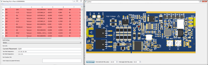
A bar code scanner is not necessary, but using one does make the process a bit quicker. When you scan a code on the part bag, the script highlights the row on the spreadsheet and puts a marker on the first instance of it on the board. After you’ve placed the part, pressing the space bar puts a marker on the next instance of the same value. The script shows it’s done after all parts of the same value are populated and you can then move on to the next part. If you don’t have a bar code scanner handy, you can highlight a row manually and it’ll tell you where to put that part. Check it out in the video below.
Of course, before you use this tool you need some prior preparation. You need a good PNG image of the board (both sides if it is double-sided) scaled so that it is the same dimensions as the target board. The parts position file generated from your EDA tool must use the lower left corner of the board as the origin. You then tell the tool the board dimensions and it scales up everything so that it can put the red markers at the designated XY positions. The script works for single and double-sided boards. For a board with just a few parts, it may not be worth the trouble of doing this, but if you are trying to manually populate a complex board with a lot of parts, using a script like this could make the process a lot less painful.
The project is still fresh and rough around the edges, so if you have comments or feedback to offer, [Colin] is listening.
[Colin]’s name ought to ring a bell — he’s the hacker who built ChipWhisperer which took 2nd Prize at The Hackaday Prize in 2014. The MeatBagPnP project is a result of having worked at building increasingly complex boards manually and trying to make the process easier. In addition to the walk-through of how the script works after the break we’ve embedded his other video from three years back when he was stuffing parts — including BGA’s — the hard way and then reflowing them in a Chinese oven with hacked firmware.


Now upgrade this with one of those picoprojectors so that it displays on your board a crosshair where your part should be.
Get a CRT , and place the board above it. Shine a electron beam from below to highlight a spot
If I understand you correctly, that might make a problem with ESD?
At least I remember my old CRT monitors as hair-raising when you put your arms next to it.
oops, I did not think about it. :(
Surely you just want the display running on a tablet, which is positioned right next to or under your board
Ya, turn up the brightness…
It would be handy for me, as I look up components in whatever PCB editor I happen to be using at the time, which is a bit laborious.
I don’t think the barcode scanner adds much functionality during placement. Currently I’m just fishing the right component out of the order box, and my eyes tell me which component it is by reading the order number. That seems to be faster.
What I was considering is making a “pick box”, where I put all components in a small box with a label. The advantage of a pick box is that it organises the process a bit more, making it faster.
https://i.ebayimg.com/images/g/ZDsAAOSww9xZGsIT/s-l1600.jpg
What I haven’t figured out yet is when the box is open how and where to label the parts.
So perhaps your program can have another row that says which box number it is in? Or a little view of the pick box that points to the box?
So yeah, good work, I may give this a try.
Try searching google for ‘smd storage box’, small comparments with individual lids you can put labels on, some even come in briefcase format!
Thanks, I found some nice ones that would allow me to fill it up once, and then create a custom “pick box” by linking them together
http://kunst.licefa-webshop.de/index.asp?katalog=0000000030&deeplink=1&shop=kunst&katalogname=Leitf26232283Bhig-28SMD29&resetfilter=1&Spalten_Unterkataloge=4&mmauspraeg1=0&mmauspraeg2=0&line=OL
http://www.farnell.com/datasheets/31299.pdf
I guess that is a solution that would help me out quite a bit.
That case is from http://www.toyourhome.co.uk/diy-screws-nuts-bolts-threaded-rods/tool-boxes/17-drawer-compartment-tool-carry-case.html
I have a couple of these: https://www.harborfreight.com/19-bin-portable-parts-storage-case-93928.html
and some of these: http://usdomainhosting.us/1449-stanley-multi-compartment-storage-box/
(I couldn’t find who’s selling these now, had them a few years…)
Seems awkward. I buy reels of resistors and caps for prototyping with the expectation of using them in production. A lot of ICs come in tubes. Are you proposing building a kit just for that build session, or a “universal” set of kits with all the various parts you buy? Cutting off pieces of tape from the reels or stripping loose 0603 resistors into the bins?
The best solution I have found for my needs is a large anti-static bin. I put all the project components in there. Decide what type of parts I’m placing first (order is often important, such as short or small parts first, connectors usually last, etc), pull that group of bags out, place each part, throw them in a temporary bin to keep them out of the way.
Yes it’s awkward, that’s why I haven’t figured out the best way yet.
Also, the concerns of the others in the replies, such as ESD safety etc.
As I’m making small series of prototype only at this stage, I use the ‘bin’ method as you describe now, but it still feels like it could be optimised a bit more.
I don’t really want to strip a bunch of 0603 resistors out into a container, because they will fleajump everywhere.
Now I’m using a magnetic saucer that catches them.
Perhaps some kind of reel holder for the more common 0603 would be handy. 10K, 100K, 100nF, 220nF
And then the rest in an ESD safe container.
When I strip a bunch of 0603 from a reel, I do it over a creased sheet of paper. When I have a few hundred on the paper, I fold it in half and funnel them into a box.
I use the SMD flip boxes linked above. I have a few hundred of them, some of them sorted by value (like resistors), and others are loosely project based, so the components that are used together will be sitting close together.
I have a pair of tweezers in my hand, and I can flip open the lid with the tweezers, and take some out. Doesn’t take more than a few seconds, and only requires one hand. The smallest boxes are about half an inch, so you can fit the entire E12 range of resistors in a single tray not bigger than a mouse mat.
I use this system to organise my collection of SMD components: http://blog.honzamrazek.cz/2016/09/the-new-way-of-storing-and-organizing-smd-components/
thanks, I’ve seen that post somewhere before, was it hackaday?
What I particularly like about the wentai boxes is that you can reorganise them later. In that way I could make a custom ‘pick box’ for each project.
I’d be concerned about ESD damage for active components.
I used to be worried about that, but I haven’t ever had any problems with that, to be honest.
On the other hand, I do try to keep things ESD safe
They sell conductive SMD storage boxes too.
Has anyone tried eevblog component folder organizer thingy?
I’ve got a DVD folder in which I stuff components and that works great if you need one single component.
But it’s not so practical when you are assembling something, because then it would require lots of flipping pages.
I have a bunch of these Stanley boxes: https://media1.bauhaus.dk/media/catalog/product/cache/1/image/800x/a0dddd2c364a3ccca80a4fdd4e04ca5b/1/0/1000738A_2_TS.jpg
I use them for slightly bigger components like Aluminium caps, plugs ect. The big thing is that you can take out each little tray an place the ones you need for the current board next to it. I put manufacturer labels on the sides of the trays, and a labelmaker label with the capacitance and footprint inside so it is visible.
Only thing is that it is not really ESD safe, but you might be able to paint them with a conductive paint?
For small SMD stuff I use proper SMD boxes. In Danish the nickname for them is “mouse toilette” :P
I do board assembly in a low-tech way: [especially for multiple boards]:
Supplies needed:
multi-color high lighter pens, post-it notes, flux pen.
1) Print [as large as practical] several copies of the parts locations & values, mark them with multi-colored highlighters [2-5 colors/parts], one color per part on the board.
2) Tin one side of each part on the PCB’s [two diagonal pins if a 4 pin or larger part], then with a flux pen, flux the pads.
3), Unzip the amount of a part from the tape needed for each part [times the number of boards],
4) With tweezers, place a part on the board with your non-dominant hand, using a soldering iron to tack it on the tinned pad.with your dominant hand [You place parts faster on multiple boards this way]. Do the same part on all the boards. After placing al the right side up parts, use a post-it note to grab the parts that are upside down to flip them over.
5) Repeat for all the parts on that placement sheet[s]
6) Check for correct placement/orientation. [easier to remove a part with only one side / 2 pins soldered]
7) Flux the pins of the IC’s on the board, then solder all the pads of the parts.
8) if appearance is important, flux all the pads, then use a heat gun to reflow the solder of the parts [surface tension will cause the parts to align themselves to the pads].
At the risk of being “that guy…”
You really ought to give solder paste and reflow a try. It dramatically simplifies the procedure.
1. Apply the paste either using a syringe to put a daub on each pad (or a stripe down the sides of ICs), or using a stencil and squeegee (a credit card works nicely – OSHStencils includes a free one with every order).
2. Use tweezers and/or a vacuum tool to place the parts. You don’t have to be too fussy, as during reflow surface tension will realign the parts as long as you’re reasonably close.
3. Place the completed board in a reflow oven and start a cycle. A reflow oven can be easily made by modifying a toaster oven to replace its control systems with something a little more sophisticated. I made my first reflow oven controller with an Arduino, an LCD shield and a thermocouple amplifier and thermocouple. For the element control, I designed an opto-isolated triac switching board, but you can also use a (suitable) SSR. It’s a project, but think of it as a Jedi assembling his own light saber.
The first time I tried it, when I was done with the pasting and PnP the board looked like a horrible mess (to my inexperienced eyes). I put it in the oven anyway and it came out looking like it had been made in a factory. Use the force.
Nick [that guy]:
If I were starting out, I would go that way, but I found that the parts shift/fall off if you look at them crooked [my prototypes/short runs some times have more than 300 parts,,and reaching across a larger board to place a part too often I have knocked a different part loose. Also, my build time may stretch across several evenings, and the solder paste dries up.- [ did my first SMD board over 20 years ago with 1206 parts, {down to 0603 and TSSOP chips now}]
My method works for me, yours works for you.
I think this is ingenious .. it’s a simple “co-bot” that can significantly speed up assembly with very low investment.
Someone above suggested using a projector of some sort to project placement spots in the board, which is neat enhancement.
I think one obvious enhancement might be to use something like zxing to scan the bar codes.
You could even have a simple enhancement that projects spots on multiple boards, if you are assembling more than one.
And the whole thing could probably be done as a web-app.
At any rate, great work.
I tend to build a kit in a 3d printed tray that I made with numbered compartments. It has ~3mm (~2/16 in) high walls between the compartments. The numbers are just 3d printed right into the tray.
Altium Designer has a documentation tool called draftsman that enables me to generate a picture of the board with BOM item numbers overlaid on the components, rather than designtators. I create a drawing sheet with this image, and the BOM.
Then I print that sheet.
This one sheet allows me to kit out the components, and quickly locate them. Sometimes if I have a lot of one component, say 10K resistors or .1uF bypass caps, I will go over them with a highlighter on the sheet to help me find them quickly.
Then I just go through my tray, starting at compartment 1, and can quickly find all item 1s on my board picture. I place them and move on to compartment 2. rinse and repeat until I’m done.
It works fairly well. I’ve done boards with up to 130 or so unique components without too much trouble this way. Breaks down a little with large components, but I find it’s usually fairly obvious where they go anyway.
>>Altium Designer has a documentation tool called draftsman
Thanks, I didn’t know about that, it looks very useful to me.
No problem, it sure beats the hell out of the old way we’d do documentation.
I actually built some templates for my company and it saves a lot of time with boiler plates notes and what not. Makes conformal coating notation, and other mechanical operations much easier to show too.
Our board stuffers love the new documentation we send them.
Large Ugly Bag of Mostly Water Pick ‘n Place
I’ve been using this for quite some time: https://www.compuphase.com/visualplace/visualplace_en.htm along with a manual pick and place contraption I built from a makeblock x-y plotter kit, a solenoid valve, a banjo pneumatic connector (so the suction tip can rotate) some steel and brass turned on the lathe, and a few other bits. Both the software, and the manual pick and place machine work well!
photo of your placement rig, or it didn’t happen! ;)
How about transparent boxes with leds to indicate which item gets placed next, ordered as you prefer to work – Cartesian or sequential or whatever.
I may have posted this before, but here’s my dream:
“Alexa, get me a 10k 0603 resistor”
“Alexa, get me a 100 nano 0603 cap”
After a series of whirring noises the component shows up in a predefined place within visual range of the microscope and I can grab it with the tweezers and place the part.
Even if it just handled chicklet resistors and capacitors that would be fantastic.
Great minds think alike
I wrote something very similar, except the barcode support.
And my tool mirrors the board image in case you place parts on the bottom side.
https://github.com/pioupus/KicadSolderTool