It is now six decades since the first prototypes of practical integrated circuits were produced. We are used to other technological inventions from the 1950s having passed down the food chain to the point at which they no longer require the budget of a huge company or a national government to achieve, but somehow producing an integrated circuit has remained out of reach. It’s the preserve of the Big Boys, move on, there’s nothing to see here.
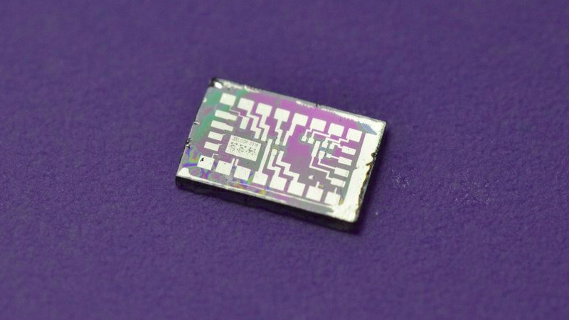
Happily for us there exists a dedicated band of experimenters keen to break that six-decade dearth of home-made ICs. And now one of them, [Sam Zeloof], has made an announcement on Twitter that he has succeeded in making a dual differential amplifier IC using a fully lithographic process in his lab. We’ve seen [Jeri Ellsworth] create transistors and integrated circuits a few years ago and he is at pains to credit her work, but her interconnects were not created lithographically, instead being created with conductive epoxy.
For now, all we have is a Twitter announcement, a promise of a write-up to come, and full details of the lead-up to this momentous event on [Sam]’s blog. He describes both UV lithography using a converted DLP projector and electron beam lithography using his electron microscope, as well as sputtering to deposit aluminium for on-chip interconnects. We’ve had an eye on his work for a while, though his progress has been impressively quick given that he only started amassing everything in 2016. We look forward to greater things from this particular garage.


This is great news! Very impressive.
Impressive!
Why can’t I live next door? Be a heck of a place to hang out, wouldn’t it? :)
https://www.youtube.com/watch?v=FiG-ZfnYkl0
I can make 747 in my garage, all I need is just few…
Jokes aside, kudos to [Sam].
If I had a garage THAT big I would not be wasting it making something like a 747. I might be wasting it *dismantling* a 747 for all the cool parts…
Project 1 in that garage:Quinnjet
Project 2: X-wing
Project 3: Millenium falcon
Project 3: Components of death star
colin furze has a few crossed off that list already I think.
Fully functioning for interstellar travel?
*Fully functioning for the 4th of July.
I think you meant 741
LM747 is a dual opamp.
He meant Boeing 747 JumboJet. It was just a light fun :D
Well, maybe you can’t make a 747 in your garage yet, but a 741 seems to be quite feasible. :)
If you could afford fuel for one long flight you could also be buying fuel and oxygen enough to put something in orbit!
Sure a intercontinental flight is split between 2-400 people but with enough hacker types, time, and 1000 patrons with $1000 could buy just about anything short of a Manhattan Project or manned escape from LEO.
Chip printers here we come!
Chips for inkjet printers made by chip printers!
The day this comes, I will record myself crying tears of joy
“Chip printers here we come!” I was thinking similar, also unobtanium long since ceased production parts … here we come.
Jerry Pournelle fan?
i thought the biggest hurdle would be the cost of the substrate
ehh, not really. I mean, it’s not CHEAP, but a wafer slice is way under a hundred, if I remember right.
Google says $5-500, depending on parameters.
It’s the lithographic plates required for modern processes that are insanely expensive, and all the intense processing that goes into it.
It depends exactly what thickness, grade, doping, polishing, etc you need – but I pay less than $20 AUD for a 4″ Si wafer. (Our research institution buys lots, though, and of course serious industrial-scale chip fabs don’t use 4″ any more because bigger wafers give better yield.)
The cost of Si is tiny compared to the equipment and labor required for the rest of the processing.
Just the cleanroom environments alone – there’s a lot of cost there, both in capital and ongoing energy.
Technically you could just directly image the chip with an electron beam… which is cheaper than a mask probalby but very slow to the point that it’s almost impractical for mass production…. 7nm at global foundries is using it though for some layers apparently where it makes sense.
I mean due to size constraints I imagine if you were going to send a chip fab to Mars … you’d send an ebeam fab because it eliminates so much other stuff in the supply chain while still producing state of the art components.
GF doesn’t use EB lithography for production. They intend to use EUV lithography for critical features combined with DUV lithography (with multiple patterning). Electron beams are very slow but are used elsewhere for masks and similar things.
EB =Electron Beam, EUV = Extreme UV (13.5 nm), DUV = Deep UV (193 nm)
Why would it be? You’re already buying a small chunk of it with every chip. Power transistors usually have the largest chunks of it, and they’re not exactly expensive.
Most of what you’re paying for is all the RND work, plus the usual operating costs any company has.
That, and the masks. If I remember right, the very complex ones (think what you’d use to make a modern CPU/GPU) can cost upwards of seven figures each, and you often need quite a few of them for a given design. But, for a hobbyist who just needs a custom ASIC and isn’t super concerned about being stick with a micron-scale process, that’s not really a concern.
The cost of a mask set on a modern process (say 48 nm and smaller) are generally said to be around a million USD for a not-too-complex process (depends on the number of metal layers and transistor types you want, more obviously requires more masks).
I can’t see much use in this though outside of the novelty (which in itself is really cool, don’t get me wrong).
same could be said for near anything featured on HaD, novelty value of hacks have a tendency to add up to more than the sum of their parts from time to time. this week for example a SDR TX hack of a USB3 to VGA dongle in conjunction with existing TV dongle hack for RX just made dirt cheap software defined radio an ineveitability. Who knows what’s next bro. exciting times on here lately :D
The substrate is very similar to the one used for (monocrystalline) solar cells.
I’ve never doubted that he would succeed, the guy is very intelligent and clearly has a lot of financial and intellectual support. I look forward to when he gets comfortable enough with the process to really push the limits of what his lab can fabricate.
Impressive work, reminds me of am radio transmitter on a chip (requiring only external dc supply, and antenna to operate) I designed and fabricated as a class project as an undergrad EE.
It was tempting to try and set up a home lab to continue working on such projects, but the sheer size and quantity of equipment to make even a rudimentary chip, not to mention the moderately unpleasant chemicals needed, put me off the project.
Wow! What a great project! Very very cool!
I knew this day wouldn’t be far off. Great job!
Hmmm, so doped silicon selective spray onto chilled plastic on the inside
of enclosures might well be the next step, not that many hurdles it seems
when you take into account the large estate available inside so many products
& for those adept at Materials Engineering who have a Chem Eng predisposition.
So who will be the first in which country to offer that as part of a mainstream product,
if not already in tightly managed robotic factories where automation at highest level
is not just the momentum but the ideal long into the future…
In before homemade SIDs. :D
I think people need to think further… Instead of just cloning existing chips, there might be applications that are unique to this manufacturing process. I’m thinking printing many layers might make it even more effective, although that leads to other issues. Can you imagine making a quick circuit in place?
Touched on this in general Joe
but, no ones taken inf further on this forum.
Have since discussed with a chem engineer how
we can do small plasma setup and the thermal
differential re chilled plastic as to what temp it
needs to be down to so we can stable adhesion
and no extraneous melting etc, First issue is
basic resistivity selective across the sprayed
layer with nodes where dopant changes etc
Anyway, here’s my earlier comment:-
Hmmm, so doped silicon selective spray onto chilled plastic on the inside
of enclosures might well be the next step, not that many hurdles it seems
when you take into account the large estate available inside so many products
& for those adept at Materials Engineering who have a Chem Eng predisposition.
So who will be the first in which country to offer that as part of a mainstream product,
if not already in tightly managed robotic factories where automation at highest level
is not just the momentum but the ideal long into the future…
@Joe: “Instead of cloning existing chips” is spot-on. If you could buy it any other way, you would. There’s no way to beat economies of scale.
My guess is that this will enable ultra-weird, custom mixed-signal chips. And that makes me smile.
This is mindboggling! Congrattulations Sam!
I hope more and more people try this, and now and then find cheaper/easier/safer subprocesses.
Perhaps we jealous bystanders should make a list of excuses why we aren’t trying this too.
If we had an explicit list of such excuses, we might try looking up or discovering alternatives.
For example, if money is the issue we flock to a hackerspace to pool resources, but in the hackerspace HF acid is the issue for insurance or whatever. I quickly googled and found a first result “Etching silicon wafer without hydrofluoric acid” although at first glance their goal was making porous silicon.
If we made an exhaustive list we might succeed in invalidating each others pessimism?
Chemicals more than anything. People tend to be rather lax when it comes to their chemicals, including disposal.
Hydrofloric Acid,
is slowly puddling in my shoe.
Bones are over-rated.
Wow, nice work Sam, can’t wait to read your writeup.
Apart from any costs involved, you must be a very disciplined person regarding how you spend your time. This kind of things need a lot of effort and most people (nowadays I include me to these people) are lazy with doing something when they are not getting paid for it. So kudos to Sam for his result!
I wonder when we will see our first 555 made at home…
it’s only a matter of time!
It’s only a time of matter
Hmm fair point, definitely going to be some delay in that, depends
of course on the capacity of those that have the power to progress
provided they can overcome the resistance and become charge
to achieve an outcome which will be illuminating, thanks for the
discrete comment by the way, its better to be monolithic and
integrated over the slab of pathways too often not pinned down ;-)
The 555 would be a perfect candidate for this, as Hans R. Camenzind designed the chip pretty much at home at his own expense :D
Too bad he will not see that happen…
Now to replicate a MOS6502!
Nice! One step closer to making our own analog neural net chips!
p.s. Is NMOS harder to make than PMOS?
You mean like: https://brainscales.kip.uni-heidelberg.de/
I made 4M DRAMs and 1M EPROMs back in the early 90s at Fujitsu. I always thought that other than alignment there was nothing we were doing that couldn’t be done DIY. even the SEM was just a QU thing most inspection was by optical microscope back then. I know that AMSAT folk have been making clean rooms with HEPA vacs and taped together plastic drop cloths. The real problem is that you have to have all of the stages ready and I recall dozens of layer and masking steps so you WILL need a well equipped fab and friends willing to work through the whole cycle which probably takes over 24 hours. At Fujitsu I remember paranoia over getting sodium ions into the gates from filthy human contamination. That and robbery of the valuable final product, they stopped packaging the chips on site after an armed robbery in ~92-93(before my time).
Operation West Chips – read to REACT formation.
More here: https://www.nytimes.com/1996/03/01/us/chip-thieves-are-arrested-after-a-sting-in-california.html
Plummeting prices have lead to specialty chips being targeted in the US: https://www.theregister.co.uk/2011/04/14/flash_heist_bust/
no word on shenanigans overseas, but one can imagine.
Hell yeah! Let’s make ICs! We can re-discover and open source all the secrets behind it.
There are some amazing people on here, when’s the first 4004 clone going to be made. ;) Seriously, that’s groundbreaking…
I would love to see a homebrew wirebonder to start using the die. :-)