Maker Faire is the nexus for all things new and exciting. At the Bay Area Maker Faire this weekend, zGlue introduced a new platform that stretches the definition of custom ICs. Is this custom silicon? No, not at all. zGlue is a platform allowing anyone to take off-the-shelf ICs and package them into a single module, allowing you to build a smaller PCB with a shorter BOM.
The idea behind zGlue is to take all of the fun chips available today from accelerometers to tiny microcontrollers with integrated wireless and put them on a tiny, tiny board that is then encapsulated. At Maker Faire, the zGlue team was busy demonstrating their cloud-based platform that allows anyone to add off-the-shelf chips to the zGlue stack and assemble it into a custom module.
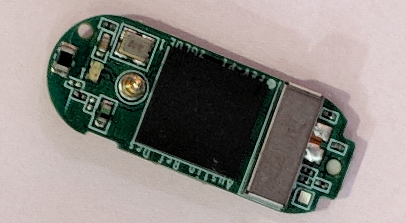
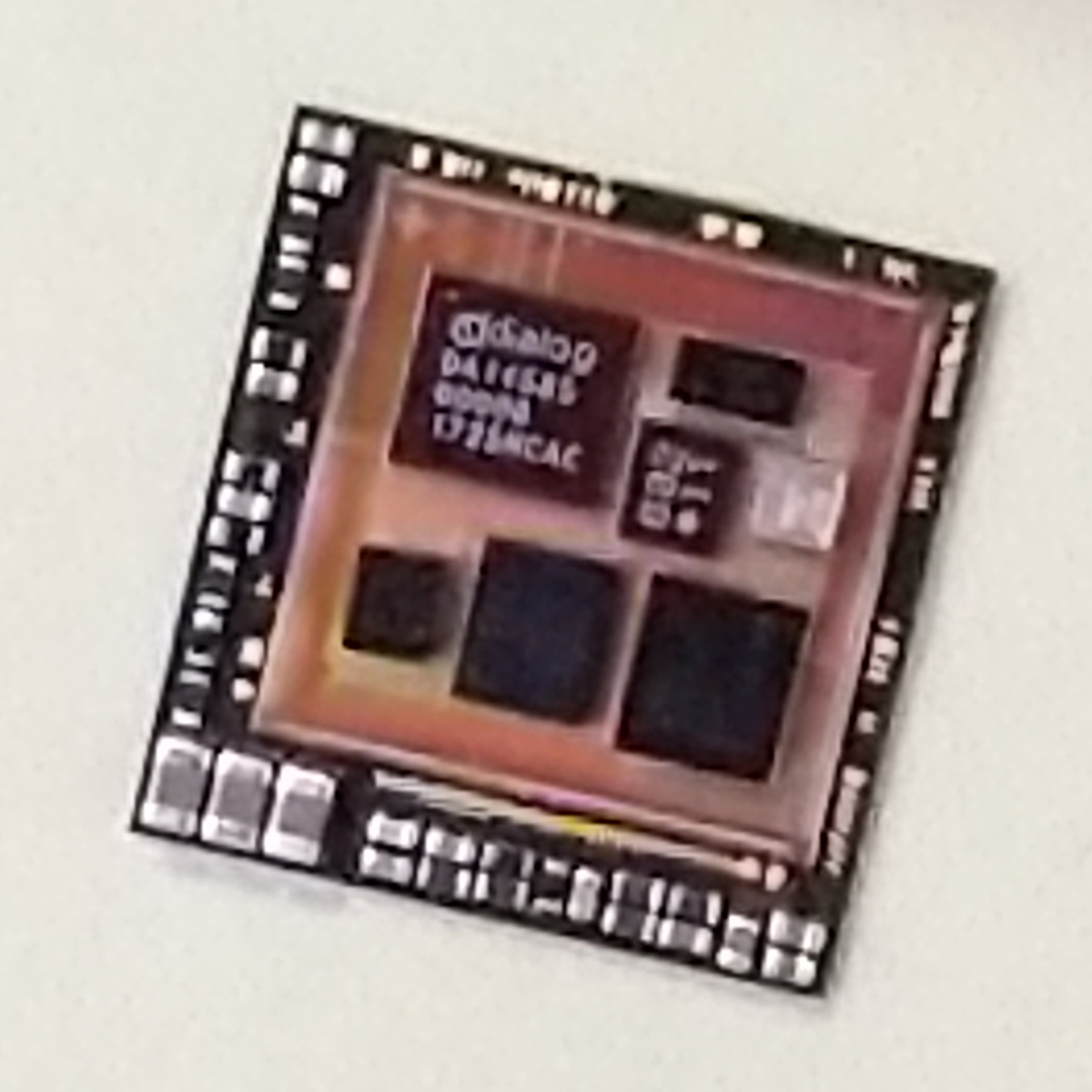
Of course, every new tech startup needs a demo, so zGlue has come up with zOrigin, a small fitness tracker that features a suite of chips crammed into one encapsulated package. The chips included in the zOrigin ZiP package are a Dialog DA14585 microcontroller with BLE, an Analog Devices heart rate monitor, a crystal, a bit of Flash, a power monitoring IC and an accelerometer. There are also thirty passives stuck in this single chip, and with a battery, some LEDs, and a vibration motor, this chip becomes a complete solution for wearable fitness trackers.
Shoving a bunch of chips into a single module is nothing new; most of wireless modules available on the market are just that. NextThingCo experimented with a Linux computer on a chip with the GR8 module, again, just a bunch of chips slathered in epoxy. The most visible benefit of custom modules is probably the Octavo System on a Chip that became the PocketBone.
While the ability to create custom modules from off-the-shelf chips is nothing new for manufacturers, the ability for anyone to create their own custom ICs has remained out of reach for the Average Joe hardware hacker. zGlue is the solution to this problem, and the prices seem fairly reasonable, starting at around $100 for the initial R&D.


how is adding a pcb using less pcb
It’s kind of like how using a dishwasher saves money even though you’re using more electricity and you’re buying an expensive detergent that cost 5 x the price of regular detergent giving you 25 washes compared to the 200 washes from a bulk pack of regular.
Marketing needs to stop at some point.
BTW you can do all these things with a 555 and a handful of 1004n’s
A dishwasher actually uses way less electricity than a human and gives much more consistent (of not spectacular) results, so that might have been the best analogy.
How do you figure?
Most humans tend to use a TON of water when washing dishes, as well as time. Time is a big factor in why dishwashers make sense, I’d argue mostly because of the opportunity cost of doing something else. But in terms of true efficiency and not just household efficiency, I’d say the reduced water usage makes it take less energy overall.
Feel free to argue, I’m not even using sources for this and if you disagree I’ll hear you out.
Maybe energy instead of electricity?
I, as a human, consume 0kwh of electricity.
You do however burn calories, which can be converted to something directly comparable to electricity use.
Hand washing externalises the cost of heating the water to another system. That may be cheap (solar heating), but mostly it will be a boiler using electricity or gas to heat the water.
It also uses a lot more of that heated water than a dishwasher that filters and reuses the water until the rinse.
Let’s not even talk about the time savings – loading a dishwasher might take some time, but it’s a lot less time than washing up and drying. If you value your time, you’ll easily make back the 15p-20p a decent dishwasher tablet costs.
A dishwasher is one of the kitchen white goods that actually makes a lot of sense.
Good point. I don’t see reduced cost either unless the ICs within were DICE/CoB and directly wire-bonded to each other – skipping the additional packaging steps for each. For a larger board where you were localizing the high layer count, blind/buried vias, etc to 4 sq cms instead of 40, maybe. But for a wearable, it don’t see the cost savings unless you are telling me they can build that interposer custom for each client cheaper than a PCB fab house doing HDI.
Because you’re effectively turning a small portion of the board into a high layer count PCB with high end fab capabilities. With many boards, there’s only a small section of the board where you’d want to have ~8-12 layers with blind/buried vias, and then everywhere else a basic 4-layer board would work. So you either make the board huge to gain routing space, or make the *whole* board 8-12 layers with high end specs. This avoids that.
Downside, as far as I can tell, is that it’ll only work with their pre-approved chips.
Also you are paying a lot more for proprietary design that you have no other control than selecting components you want. No way to know, if they don’t screw up the routing. Also if they fail as a company (which they will), you get screwed too, and have to redesign your thing at a cost.
Also if you need 8-12 layers, you can design your own minimodules, order them manufactured and use with 2-4 layer main board.
And another point – there are plenty of fitness trackers that are very small and compact with 4-layer PCBs without using “zBullshit”…For example Garmin Vivofit 3 (tiny package), Jawbone Up bands (bad flex-pcb design that caused them to break easily), etc…
There is a huge lack of real information on their website but it seems their “interposer” is actually a chip (then mounted on a PCB). They talk about a “silicon platform” and features such as power management, security and level translation. I guess they are adding a programmable interconnect and array of connection points on top to match those of the silicon application chips. That would explain why they would have to have a library of supported chips. It’s an interesting idea (I like the ability to probe the interconnects between chips) and will be cool if they really could deliver you prototypes for $100 (+ parts? + other?) and have a useful library of supported chips.
Shouldn’t they first be de-capping the original chips, and re-bounding them to the new package? That would make much more sense.
Imagine getting a batch of 100, with 5 ICs in each, thats’s 500 ICs to decap, and tens of thousands of wires to rebound. It’s also something you can’t automate, unlike pick and placing IC’s.
Some chips come in CSP which is easy to bond to another substrate, and others can be bought directly from the vendor in bare die for exactly this purpose.
That would be a nightmare.
Dad was mentioning the other day old aerospace stuff where they’d do this with bare dies and a wirebonding machine with the milspec equivalent of 74-series logic chips.
At a previous job I helped update a datasheet for a communications ASIC to include info on whole wafer “packaging” for a military customer.
My guess is they wanted to do more stringent ATE die probe testing than we were doing before putting parts into… whatever. Maybe they bonded it into an MCM, maybe they did their own discrete packaging.
They also do just that with the very cheapest chinese-made toys. Wirebonding bare dies and encasing it with a blob of epoxy seemingly is cheaper enough to make it worthwhile.
Reminds me of thick film hybrids we used to build on the early 80s, except there was a real need for thick film hybrids.
We were still making those in the late 90s at a large automotive company I worked for. I started there doing layouts for hybrids in 1989 and then writing design automation software. About 10 years later we were spun off as a separate company (which totally sucked in many ways) About the time of the IPO I had moved to the IT department, and at some point, after that, all the manufacturing moved overseas. It was a great place to work for a while at least. I took an early retirement in 2006, a few months before they laid off all of the IT department (very stupid). Bankruptcy (for them) followed.
That’s what came to mind. What’s old is new again. Next thing you know COBOL will be making a comeback.
I think it’s pretty cool, not everyone wants to invest in all the equipment to be able to reliably create things at that tiny scale for small quantities (not the millions of devices a large company would make).
I wonder what the minimum order quantity would be beyond that $100. If you could make say 10-20 of something I think it would be epic for the kind of products you find on Tindie these days.
And for that money you get a big chunk of your product designed by someone who knows their stuff (supposedly anyway).
And of course, you could always have them make you a module with LMC555s (a 1.43mm x 1.41mm 555 timer) + passives if you wanna be a true Hackaday Comments Wizzard.
COBOLOC
COBOL On a Chip!
Looks like a lot of hype so far. Lots of flashy video and PR, but no sign of how the service will work, pricing details such as order minimums, logistics on how chips are supplied (T&R only?), etc. The specs that are available aren’t that impressive (.2mm pitch supported).
small brain: wafer in blob on board
bigger brain: wafer in casing on board
galaxy brain: wafer in casing on board in casing on board
Really though this could be neat.
And if you want control over the PCB layout – heat dissipation, groundplanes, high-speed digital interconnects with length matching, high-current power interconnects, or impedance-matched RF transmission lines, then suddenly you’ve lost that. Not all wires are abstract and fungible.
Looks interesting on first sight, but as others mentioned, there are a few details missing here that could help make this something useful to me and my company. One of the bigger issues i see coming from an industry having product life cycles between 10 to 20 years is long term availability. I don’t think they can offer any guarantee that as long as the individual chips are available from the manufacturers they would be around to assemble them into modules. So, we’ll just do what we did before, make our own highly integrated modules (where we have the control over layout, function and data in house) to slap them on to the standard PCBs with all the larger components…
Or for larger numbers, just go directly down the custom SoC or ASIC path.
HaD said: “the ability for anyone to create their own custom ICs has remained out of reach for the Average Joe hardware hacker. zGlue is the solution to this problem, and the prices seem fairly reasonable, starting at around $100 for the initial R&D.”
C’mon HaD. That’s ALL you can say? I get that from the Marketing Hype from the company direct. So NO real numbers. And YOU HaD just parrot the LACK OF INFORMATION.
What do I come here for HaD? Information of course! That’s what you get paid for HaD – right? In this case you provided NOTHING new or insightful about this new offering any of us can get in a short amount of time ourselves.
You have Journalistic CLOUT HaD that we the small people do not. Why didn’t you use that clout to dig further and tell us what you found (or tell us of the company told you nothing)?
Typo: (or tell us of the company told you nothing)? => (or tell us IF the company told you nothing)? Sry…
And that’s another thing HaD, where’s the comment editor? Make it work for at least 60 seconds before lock-out. It’s been YEARS since you finally let us post caps in comments, and it’s been YEARS since there’s been no progress since. Still no comment editor HaD?. Sheesh.