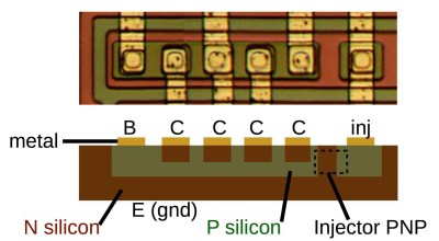
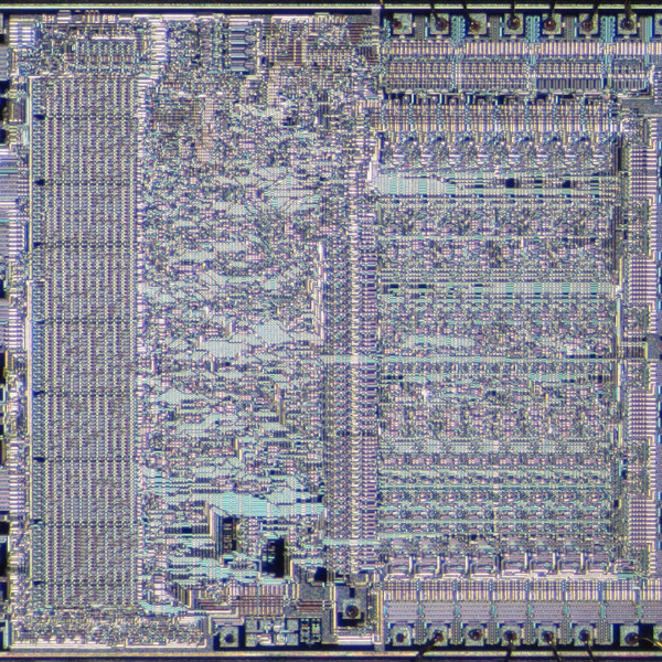
It must be everyone’s birthday today because [Ken Shirriff] has come out with a gift for us. He’s done another pass at reverse engineering the 76477 Space Invaders sound chip from the 1970s and found it’s full of integrated injection logic (I2L), making it a double treat: we get to explore the more of this chip which made sounds for so many of our favorite games, and we explore a type of logic which was to be the successor to TTL until CMOS came along.

This article has a similar shape to his last one, first introducing I2L, followed by showing us what it looks like on the die, and then covering the different functional elements which make heavy use of it. The first of these is the noise generator made up of a section of shift registers and a ring oscillator. That’s followed by a noise filter which doesn’t use I2L but does use current mirrors. And lastly, he talks about the mixer which mixes output from the noise generator and elements covered in his previous article, the voltage-controlled oscillator, and the super-low frequency oscillator. Oddly enough, and as he points out, it isn’t an analog mixer. Instead, it just ANDs together the various inputs.
[Ken’s] no stranger to putting dies under the microscope. Check out our coverage of his talk at the 2016 Hackaday SuperConference where he shows us the guts of such favorites as the Z80 and the 555 timer IC.


Does somebody know good resources like tools, howtos… for reversing doublesided pcbs?
I’ve got an old desk calculator with nixie tubes from about 1970 and I would really like to get the secrets out of this device.
https://meta.it-syndikat.org/t/commodore-1161-restauration/1284 (sorry, it’s german – but mostly photos)
I was wondering if “restauration” was a portmanteau of restaurant and restoration.
B^)
I don’t know any specific tools, but a good place to start is imho to just take your time and start digitizing away. If you get nice pictures, like on that website, they can be used as preliminary “checklists” to make you you don’t miss a component or connection.
My guess is there are no tools you can just feed a picture and it converts it back into the schematic and layout files with a spark of magic math power. It takes a lot of manual work to create netlists, find every single parts function and value, and then figure out the design intent behind the chaotic schematic you would get when you actually did get every connection and part correctly.
As long as the pcb is not to fine/complicated my simple tool for reverse engineering a pcb is a bright desk lamp. PCB materials where/are somewhat transparent to light. The traces become shadow lines.
To add in some additional detail to the other posters – some time ago someone mentioned imaging both sides othe PCB and then overlaying the image. I suspect that you could do a couple different things with that:
-> Keep them both as layers /discrete images and rotate them so they are both “up” (whatever that means to you, so long as it’s consistent) and flip back and forth between them while taking notes. If you line them up really well and keep a mouse/arrow key available to exchange the images, you should be able to rely on your short-term memory and even (to some degree) “persistence of vision” to help you correlate components and paths on each side.
-> Alternately, fire up you favorite image editor, overlay the images, and make the one on top 50% transparent (to the eye) or something like that. Then you can really see both layers at once.
-> If you really want to party, do as above but then get your image editor’s line tool out, make a new layer, and trace circuits of interest – for example, you can trace the flow from Vin through the power conditioning circuitry and then down into the rails on all the individual ICs. Or you can start at the serial port and trace back to the ICs it talks to. Keep ’em all on separate layers so you can mix/match as needed, then overlay when you reference that specific part!
As for image acquisition, I’ve heard that flatbed scanners can have poor depth of field, so a camera (in RAW, if possible!) would be a good choice. Get dat maximum effective resolution, otherwise you might have weird compression artifacts making your life difficult.
This is what I’ve done. I first takes as many pictures as possible,and try to determine what the components are (datasheet,if possible).
I’ll typically remove what components I can just to get a bare PCB.
I use a copy machine to get images of the top and bottom, once I have images, I draw the symbols on the paper.
I’ve used GIMP or some other software that allows me to have layers.
So,with pictures of top and bottom, symbols drawn, I can now build a schematic. A rough one at first,but once it’s drawn in software I can move stuff around to make more sense of what’s doing what.
From there, I create a PCB,trying to get components and traces the same size, location, direction of the original.
If all works out, everything is correct.
I’ve successfully reverse engineered many PCBs this way, though getting success from multi layer PCBs and surface mount is extremely difficult.
With those, I’ve had success but not without loosing my hair.
I’ve also seen someone take an image file and convert to DXF or DWG. From this,a gerber can be created.
This last mention works but there are certain combinations of software that work and those that do not….