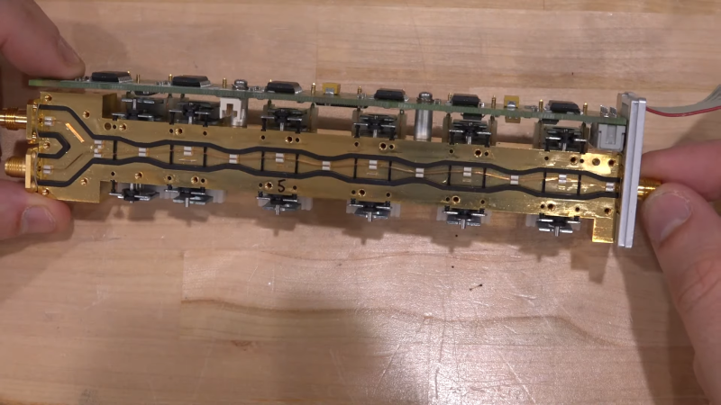
It might not count as “DC to daylight,” but an electromechanical attenuator that covers up to 70 GHz is pretty close, and getting a guided tour of its insides is quite a treat.
Perhaps unsurprisingly, this one comes to us from [Shahriar] at “The Signal Path,” where high-end gear most of us never get a chance to work with goes for one last hurrah after it releases the magic smoke. And indeed, that appears to be exactly what happened to the Rohde & Schwarz 75 dB step attenuator, a part that may have lived in the front end of one of their spectrum analyzers. As one would expect from such an expensive component, the insides have some pretty special engineering. The signal is carried through the five attenuation stages on a narrow strip of copper. Each stage uses a solenoid to move the strip between either a plain conductor or a small Pi pad with a specified attenuation. The attention to detail inside the cavity is amazing, with great care taken to maintain the physical orientation of the stripline to prevent impedance mismatches and unwanted reflections.
The Pi pads themselves are fascinating, too, especially under [Shahriar]’s super-duper microscope. All of them were destructively removed from the cavity before getting to him, but it’s still pretty clear what’s going on. That’s especially true with the 5-dB pad, which bears clear signs of the overload that brought on the demise of the whole attenuator. We suppose a repair would have been feasible if it had been just the one pad that needed replacement, but with all of them broken, it’s off to the scrap bin. Or to the recycler — there appears to be plenty of gold in there.
We thought this was a fantastic look under the covers of an exquisitely engineered part. Too bad it didn’t rate the [Shahriar] X-ray treatment, as this multimeter repair or this 60-GHz phased array did. Oh, well — maybe next time.


Pi pad and no further explanation of what that is..
From Wikipedia, the free encyclopedia
The Π pad (pi pad) is a specific type of attenuator circuit in electronics whereby the topology of the circuit is formed in the shape of the Greek capital letter pi (Π).
I must admit I did not expect to see one of these gracing the pages of the Hackaday blog. This is an edgeline step attenuator which I used to design many years ago. (I’m not the same person who commented on this in the YouTube comment section).
The edgeline impedance is controlled by the gap between the ribbons and the side of the cavity which makes it ideal to switch between two paths in the Z axis over a wide frequency range from DC to XGHz.
At the time most spectrum analysers and signal generators would go down to 9kHz so ‘DC’ performance was a must.
The ribbons are held in place in this case with thin tubes of dielectric. You can’t have a substantial plastic support as the ribbon has to neck down to keep the impedance constant. This leads to a weak point in the ribbon which causes fractures over repeated usage.
The ribbons are made from chemically milled tempered beryllium copper which has the necessary flexibility but without the work hardening of pure copper.
The plating on the contacts was very difficult to get right as the slightest contamination would form an oxide layer which was an effective insulator at the very low signal powers that step attenuators normally switch. A layer of a few atoms of a hard oxide like Tin would form an impenetrable barrier. So called ‘pure’ plating solutions turned out to be anything but pure.
The electromagnetic actuators are bistable magnetic circuits with fixed magnets between two C shaped steel plates.
The upper frequency is determined by a number of factors including the waveguide frequency of the cavity. We always tried to push this up as high as possible but the trade off is in the size of the parts.
Cavity isolation limits the overall maximimum size of the attenuator although at lower frequencies it was possible to have more sections.
The pads are normally made using a thinfilm process with something like Tantalum Nitride as the resitive element. Most designers used alumina or sapphire as the substrate.
The most common form of destruction was somone connecting up a PMR or tactical radio to the spectrum analyser and then hitting the PTT key, although failure from long term contamination was another problem.
The design in the video is very similar, one might almost say identical, to the original Anritsu (formerly Wiltron) design in all respects where the cavity is split vertically.
The alternative design used by a number of other manufacturers split the cavity horizontally so that the attenuator pads were held in a separate holder which then mated with a machined cavity and ribbons.
The advantage of this design was that the width of the cavity was controlled by a single machining operation on a single piece of metal.
These things were extraordinarily difficult devices to get working properly. The basic principles look quite simple but the devil is in the unseen detail. I learnt a lot the hard way about a huge range of engineering technologies under the pressure cooker of getting reliable product out on time. But that’s a story for another time….
Thanks for taking your time to share – very interesting.
Hahahaha 70GHz attenuates even by thought!
It’s enough some meters of mist to attenuate frequencies like that!
the production of this piece is my daily work. Thank you for this appreciation.