
The first thing I ever built without a kit was a 5 V regulated power supply using the old LM309K. That’s a classic linear regulator like a 7805. While they are simple, they waste a lot of energy as heat, especially if the input voltage goes higher. While there are still applications where linear regulators make sense, they are increasingly being replaced by switching power supplies that are much more efficient. How do switchers work? Well, you buy a switching power supply IC, add an inductor and you are done. Class dismissed. Oh wait… while that might be the best way to do it from a cost perspective, you don’t really learn a lot that way.
In this installment of Circuit VR, we’ll look at a simple buck converter — that is a switching regulator that takes a higher voltage and produces a lower voltage. The first one won’t actually regulate, mind you, but we’ll add that in a future installment. As usual for Circuit VR, we’ll be simulating the designs using LT Spice.
Interestingly, LT Spice is made to design power supplies so it has a lot of Linear Technology parts in its library just for that purpose. However, we aren’t going to use anything more sophisticated than an op amp. For the first pass, we won’t even be using those.
How’s it Work?
Inductors and capacitors are energy storage devices. In particular, an inductor stores energy as a magnetic field and responds to the change in the current through it. The idea behind a switching buck converter is to pulse width modulate the current to an inductor so that it produces the desired voltage. You’ll also want a capacitor at the output and you need a way to shunt negative voltages caused by reverse current flow to ground such as a Schottky diode. A typical architecture looks like this:
You can find the whole thing on GitHub. Notice that here, I’m using a Spice voltage source for the input voltage and a pulse generator to create PWM. You can set the period with parameter T and the duty cycle with parameter D. I didn’t do a lot of logic picking components here. I pretended I was digging through my junk box and grabbed the first things that seemed like they’d work. If you want to maximize efficiency or minimize startup time or optimize anything else, you probably should work smarter than that. The frequency I picked was arbitrary — about 333 kHz. Again, I just wanted a circuit you could experiment with and we’ll build the rest of the circuit around this core.
If you experiment a bit with changing D, you can probably intuit a great deal of what the mathematical analysis will tell you. Over at least some range of operation, the voltage out will be roughly the voltage in multiplied by the duty cycle. If you want a 5 V output with 15 V in and your diode and other components are perfect, the duty cycle is 1/3. Of course, your diode will have some drop and the other components have parasitic elements, so the reality is it will be a little off at 1/3. Try changing the diode model to ideal and see how that affects things, or try a silicon diode. You can see I have 0.31 and that gets pretty close.
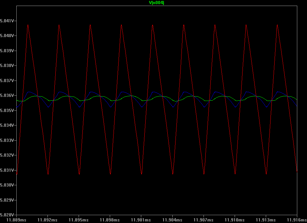 Try removing the diode. You’ll see the voltage at the transistor’s source will go negative. You’ll see what effect varying the inductance value has in a bit. Try changing the capacitor’s value and note the effect — especially on startup time. This is one of those cases, too, where the capacitor’s ESR (effective series resistance) has a major effect on circuit operation. If you right-click the capacitor, you can add a little ESR. Try 1 Ω — high for a ceramic capacitor but not so high for an electrolytic — and note the effect it has. At first, you might think it doesn’t have much effect, but zoom in on the output voltage once it is stable. You’ll see the ESR adds ripple to the output. The green trace is 0.01 Ω, the blue is 0.1 Ω, and the red is 1 Ω.
Of course, the inductor and capacitor also form a resonant circuit which can interact with the PWM frequency, but for now, I am literally just “junk boxing” the circuit so we’ll skip the math. The frequency of the components shown is just under 2 kHz. Try setting the T parameter to 1m (1 kHz) and see what happens.
One of the nice things about this circuit is the transistor is either on or off. Since a MOSFET will probably have a very low on resistance it won’t dissipate much power. This allows switchers to operate much more efficiently than using a pass transistor as in a normal linear power supply. Of course, the switch doesn’t have to be a FET, but FETs work so well that it is rare to see anything else used in a modern design.
However, this does mean low on resistance is important for efficient operation. Note I am driving the gate at a higher voltage than the supply voltage because I wanted the maximum Vgs for this device. This isn’t always necessary but since the source voltage will be roughly the drain voltage at some point, it is a good idea or else efficiency will suffer or the converter may not work. In real life, the difference might not be as great as I use here — maybe a diode drop or two, if any.
Again, this is just to get a feel for the circuit. In the final design, we probably want some resistors to snub any high frequency oscillations and take care of some other practical concerns. We could make changes to increase stability, efficiency, size — but probably not all of them at once. For example, adding a snubber has advantages, but will decrease efficiency. But for now, this will get us started.
Modes
 Notice when I was talking about duty cycle setting the output voltage that I said “at least some range of operation?” It turns out there are two different regimes this circuit can operate in. In one, the current in the inductor will fall to zero at some point. This is discontinuous mode and is harder to handle because almost every component will play a part in determining the output voltage.
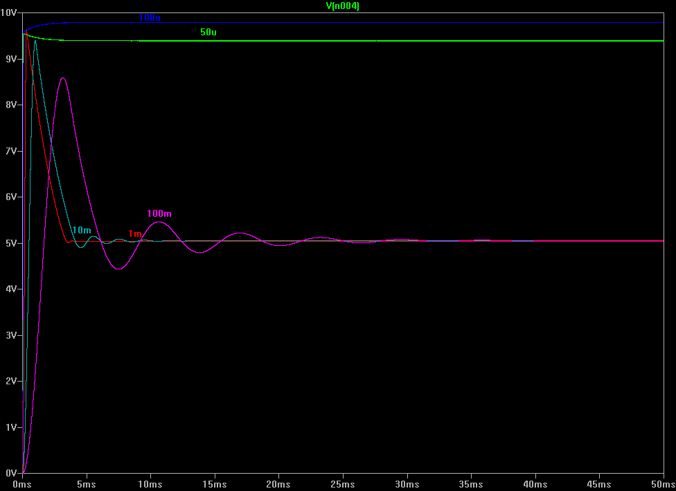
However, if the inductor current does not go to zero, the output is purely a function of the duty cycle. That’s generally the mode you want, so you’ll want a larger inductor. Right now, the inductor is 1 mH and the inductor current stays between 5 and 15 mA if you let it stabilize. Try, say, a 50 μH inductor. Here are some plots showing output voltage with inductors ranging from 50 μH to 100 mH. You can see the lower value inductors are not in the operating regime we want.
Why Stop?
A lot of tutorials will stop here. The problem is, this isn’t a regulator. If the input voltage goes to, say, 10V, what happens? Or 20V? The problem is the 1/3 PWM duty cycle only works for 15 V. What you want is a servo loop that compares the output voltage to some reference and generates PWM based on the difference.
That doesn’t make sense at first. To make a 5 V supply I need to compare it to a 5 V reference? There are two things to consider. First, it is relatively simple to make a precise voltage reference that can’t handle a lot of power. For example, a diode or LED drop is pretty constant over a wide range. A Zener diode can work too but isn’t good for power applications. You can make a low-current reference voltage much easier than a power regulator. The other trick is to use a voltage divider to sample the output voltage. So maybe your 5 V output produces 1.4 V after the divider and you compare it to two diode drops. Now it makes more sense.
The answer, then, is to figure out how far the voltage is from what you want. Then you can create a PWM signal to control how often to turn on the gate of the transistor. If the output voltage is OK, you don’t need to do anything. If it isn’t on target, though, you need to change the PWM drive. Block diagram-wise:
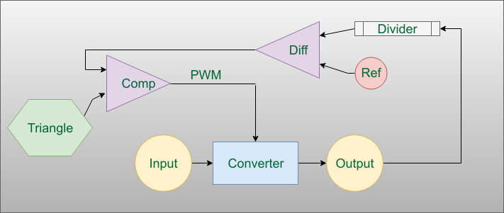
The converter is just the part we saw earlier. The divider is optional but should get the expected output (5V in this case) down to the reference voltage, whatever that is. The output of the differential amplifier is the error voltage that mixes with a triangle wave in the comparator to generate the PWM at the correct duty cycle.
PWM?
If you are wondering how a triangle wave and a comparator generates PWM, this picture should clear it up:
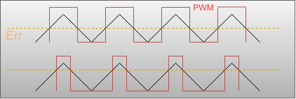
The black is the triangle wave, of course. The yellow dashed line is the error voltage. The comparator output (red) turns on when the triangle is higher than the error voltage. In the top trace, the error is about midway so the output duty cycle is about 50%. In the bottom trace, the higher voltage creates a lower duty cycle. If you need to reverse the action you can do that by flipping the comparator (or flip your monitor; we’ll wait). That is if the comparator goes low when the error voltage is higher than the triangle wave, that will have the effect of inverting the red square wave making the duty cycle inverted.
Now, this raises another question: how do you generate a triangle wave? There are a few ways to do that. The classic way is to take a square wave that goes from positive to negative and integrate it. You can also take advantage of the fact that a constant current source will charge a capacitor in a straight line. A constant current sink will discharge it the same way.
You can see why an integrated solution is popular. Having the closed loop control not only provides regulation for changes in input voltage, but also — if the reference is good — for variations in components, temperature, and load currents. However, the circuitry does get a little complex. Keep in mind, too, I’m trying to make a quick and dirty simple version. There are all sorts of tricks people use to get better performance — depending on how you define performance — and I’m ignoring all of those, at least for now. But that makes the complexity even greater.
Also, this is just one topology. Some buck converters will use two FETs. Some will reduce switching frequency based on load. Then there are boost topologies for going from a lower voltage to a higher one and even boost-buck when you just can’t decide.
We will flesh out the design more next time. We’ll eventually get to a buck converter that regulates.


> LT Spice is made to design power supplies.
Nooooo. It’s made to simulate power supplies. Simulation =/= design.
Well, I hate to be as pedantic, but I think of design as a lifecycle and yes, that includes testing via simulation and via real word testing, too. I think a lot of the projects I’ve worked on that have been less successful were burdened with that sort of thinking (throw it over the fence). I designed it so it is done! The modern shift to looking at a cyclic design flow has been a good thing. Same for FPGAs. Part of your design workflow is simulation. Now, I’ll take your point that simulation doesn’t have to be a design activity — sometimes you are trying to figure out why something failed or isn’t behaving. But I’d suggest that if you are, then your design activity failed to start wtih, more than likely.
It does not matter is something you dreamed up in your head or formally laid out in a program like SPICE, simulation is a critical part of design. I believe this is a great article that focuses on that part of the design process.
Dreaming as a form of simulation? Interesting.
Wahhh!
it’s 2018, simulation is an essential part of a good design process.
Yes, simulation is part of the design process. I didn’t say it wasn’t, so was surprised when multiple posters felt the need to “correct” me.
I use it too, in multiple domains, and have done so for decades. On occasions I have even written my own simulation software.
But one should never use simulation as a replacement for understanding, and one should not think simulation *is* design. I contend that’s true for my domain (circuit design in communications products) but I understand it may not be true for other domains (e.g. neural nets, where we don’t have a really good understanding of what’s going on and simulation is the only way to “design” anything).
I think he meant LM309K, a TO-3 5V regulator that needed a massive heat sink for 1A when driven from 12V
Yup. 390 was an audio amplifier. Well… I had all the right digits.
Thanks. How about step up converters, is that another story for another day? My (limited) understanding is that they are essentially the same thing except for the way they switch.
Probably won’t be the next one, but yeah we’ll get there.
A couple more questions: why not use a PN diode, is it because of its voltage drop? And why does the cap ESR have so much effect, isn’t it just equivalent to the load resistance being very slightly more?
Lower forward voltage and shorter recovery time are why Schottky diodes are used more often in switching regulators.
These both contribute to higher efficiencies in the design.
No because the ESR is in series with the capacitor not the load. It shunts the load. So the way to think of it is the inductor current through that resistance creates a little battery going up and down across the load.
You might enjoy this:
https://pdfs.semanticscholar.org/presentation/df9a/e116d5c2dc65c8f5225c3e975c94aa68e726.pdf
Ah, ok, thanks guys for the clarifications.
I have done a hysteretic buck converter design + prototype in my hackaday project page. It comes with documentation, LTSpice simulation file, actual measured waveforms etc. All of the trial & error work is done in LTSpice before prototype and that saved me a lot of time.
https://hackaday.io/project/2145-smps-replacement-for-7805/log/36375-discrete-33v-buck-converter
Great link! Nicely done.
“Inductors and capacitors are energy storage devices. In particular, an inductor stores energy as a magnetic field and responds to the change in the current through it. The idea behind a switching buck converter is to pulse width modulate the current to an inductor so that it produces the desired voltage. You’ll also want a capacitor at the output and you need a way to shunt negative voltages caused by reverse current flow to ground such as a Schottky diode. A typical architecture looks like this:”
My eyes are bleeding.
Falstad would be a much better tool for beginners to visualize what is happening.
The flyback diode provides a return path for the current through the inductor so that the inductor can discharge when the MOSFET switches off.
While the ESR of the capacitor is important [to output ripple], many SPICE models give odd results if you neglect the ESR of any inductors in the circuit.