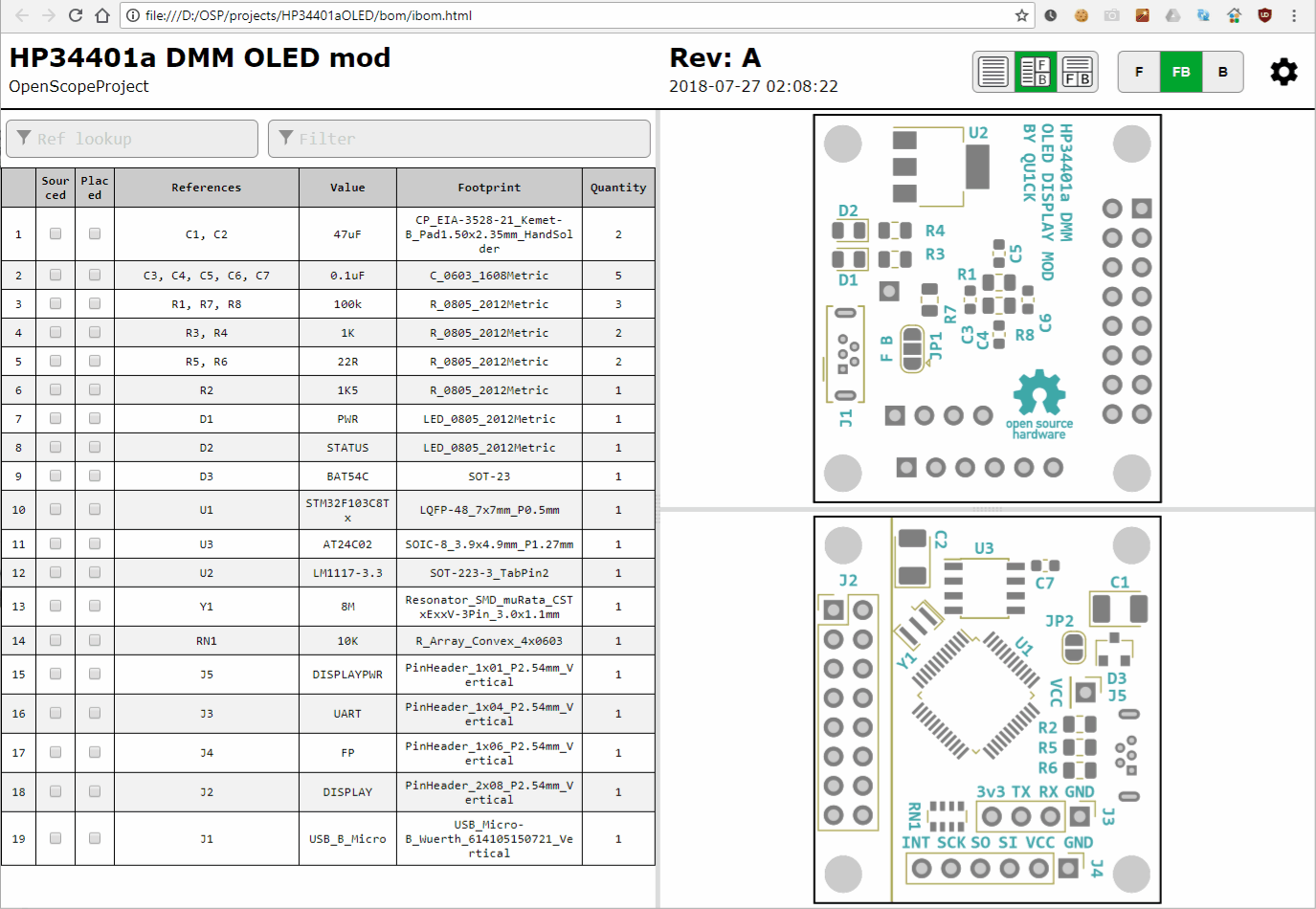
We’ve all been there; you finally get the last DigiKey box and now your desk is covered in parts to stuff into a shiny new PCB you’ve been working on. First stop? Passive town, population endless waves of 1uF capacitors. The first one goes in the upper left, then a little below that, then… once you get to C157 it’s getting pretty hard to remember exactly which parts go where. Enter the literally named InteractiveHtmlBom (IHB) to smooth this process out.
IHB makes the frustrating task of mapping lines in a BOM to a physical position on a board easy. The classic method is of course, to look at the BOM, then search the board for that designator and place the component. (You left the designators in the silk, right?) Or to look at the BOM, ask your CAD package to search for that part in the layout, then place. IHB generates a document that does this automagically.
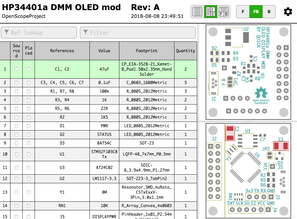
Run the tool, either standalone or as a plugin for KiCAD 5.0, and you get a folder with the new interactive BOM in it. There are a few view options but generally it presents a view of the BOM with designators and value in one pane and a wonderful render of the top and/or bottom of the board in another pane. When you hover over a BOM line it highlights the relevant parts in the board view! There are toggles for filtering by top and bottom of board, marking which parts have been placed, light and dark mode, etc. Plus the ability to filter and sort by designator and value. We would have been impressed if it was just a generator/viewer for those slick scrollable/pannable board renders!
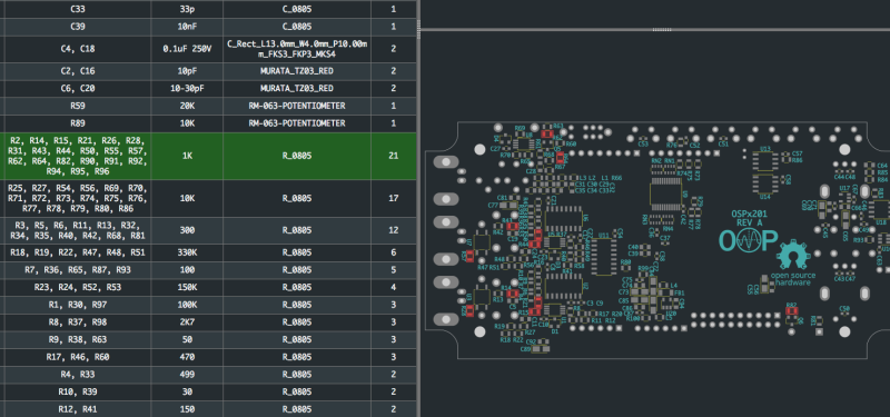
Check out a very long GIF demo after the break, or explore one of many pre-created demo BOMs here. We’re partial to the OSPx201.
Thanks [GregDavill] for the tip!


That’s fucking cool. I think my fab house / assembly guys would wet themselves if I sent this along with BOM and assembly docs.
KiCAD is quickly becomming a flagship FOSS project, like firefox, gimp, blender, VLC, it’s starting to boast features that compete/surpass with expensive professional commercial software. Appreciation to Wayne, developers and community, and CERN for pushing things forward on this tool.
Anyone thinking of learning KiCAD should check out contextual electronics by Chris Gammel, he has a free concise tutorial series called ‘getting to blinky’ that’s like the hello world of PCB design. goes from a schematic diagram to a physical prototype in a couple of hours.
I fully agree with you there, we’re engineer’s and hackers not sailors (even then I bet you can find more than a few of those that can keep their tongues in check).
The dean of my community college would swear up and down left and right… it was highly unprofessional. Moving on to a 4 year school, I don’t remember anyone there cussing not once… that said I generally just tune it out, since about half of people do it.
My grandpaw back in the 80’s stood up during on of the parents meetings at a local state university and expressed his concern with alcohol on campus and in the dorms… apparently most parents cared more about thier kids getting liquored up and having a “good” time than getting a good education. This was much to the detriment of my parents education who took school seriously and had to deal with the drunken parties of soon to be drop outs.
“it’s starting to boast features that compete/surpass with expensive professional commercial software”
No.
It has some features that are exclusives. It doesn’t have some other features…
That looks awesome! Haven’t played with KiCAD in ages (seemed very primative at the time), will have to give it a try as it looks like it has had a lot of developments. When stuffing a board I’ll usually print out the silkscreen designation and pad layers for each side along with the bom list and highlight/cross out components as I go along so I can keep track of progress. I assemble in terms of modular functionality and test each part successively and every test is documented and checked off before going on to the next. The interactive BOM looks like a step closer to digitizing this ritual to appease the magic smoke gods lest all the electrons fall out.
Looks cool. I’ve usually just put a small font for the “value” labels and printed an assembly drawing with them visible: https://jpa.kapsi.fi/stuff/pix/assembly_info.png
Around 1990 I did an internship at a small company where PCBs were populated and soldered by a small team of ladies. The company had a special workbench for populating circuit boards that had a multi-layer carousel with small trays of parts, and a device that would project a small rectangle of light on a PCB where the part needed to go. I’ve tried to find information about these machines online but they’ve been forgotten in the pre-World-Wide-Web darkness. Would be nice to have (make?) a machine like that, in combination with this plugin, to help you populate circuit boards.
Not quite the same, but I’ve seen similar systems in user for composite layup
An example: https://www.lap-laser.com/general-industries/projection/laser-projectors/composite-pro/
Your link is confused, it should be https://www.lap-laser.com/general-industries/projection/laser-projectors/composite-pro/
Haha, thanks!
This goes into a similar direction: https://hackaday.com/2018/07/26/bringing-augmented-reality-to-the-workbench/
My aunt used to assemble security system boards here in the USA… she’s does medical coding these days (billing not programming, though it may as well be as complex as it is).
It probably used the Gerber files and an aperture to match the size of the part? That seems pretty straight forward.
That’s an interesting point, it could literally be an X/Y plotter moving to coordinates…. hm!
You are referring to a Contact Systems CS-400 machine or an earlier model. Quite common in those days.
This piece of free software does something similar if anyone’s interested
http://www.alciom.com/en/downloads/free-downloads/123-smtassistant-software.html
Habatchii says;
Very well. The guys at CubeSat will appreciate the updates.
Again, very well…
https://www.compuphase.com/visualplace/visualplace_en.htm
Is what I use… it imports kicad output as well.
Ditto. I also use VisualPlace for every board I build. It uses the gerbers and .pos files (created by KiCAD as well as every other decent tool) to do the dirty work so isn’t tied to KiCAD. It has more advanced camera stage driving functionality I don’t need (and clearly haven’t read up on yet) which I believe can automatically shift a camera or the board so you don’t even need to touch it as you work down the BOM!
If only a tool existed that went the next step and sorted the parts into ‘little ones first’ order to make assembly even easier (I just do it manually, but I rarely assemble more than five PCBs a week)
This is a good path for KiCAD to gain a broader audience. In “real” manufacturing, software programs from Aegis (Fusion and Factory Logix) and Mentor Graphics (Valor) do exactly this without blinking an eye. There are also a ridiculous number of other features for manufacturing, single piece to high volume, that will never exist with KiCAD.
I can see some good uses for that, coupled with an usb pedal to jump to the next component in the list
MIDI pedal even better!
The airturn BT200/S2 might be a good choice (Bluetooth + MIDI).
It would be great to make this a generic tool as well! Via Gerber and XYRS Files, or perhaps with ODB++. That way all of the EDA tools could play nice!
exactly what i thought…
I’d like a voice interface – so I can say R12 or “next”.