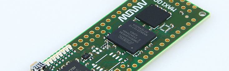
Ok, we’ll admit it. We like FPGAs because it reminds us of wiring up a 100-in-1 kit when we were kids. But the truth is, many projects are just as well off to have a CPU. But there’s a real sweet spot when you have a CPU and an FPGA together. Intel (or Altera, if you prefer) has the NIOS II CPU core, but that’s hard to configure, right? Maybe not, thanks to a project by [jefflieu] over on GitHub. He’s assembled some basic definitions and libraries to easily — relatively speaking — use NIOS II on the MAX1000 as well as a few other boards. The MAX1000 is a pretty nice board for about $30, so this is a very inexpensive way to get into “System on Chip” (SOC) development.
[jeff] goes into more detail in a blog post, but the idea is pretty simple. We tried it, and it works very well, although we found a few things hard to follow so read on to see how we managed.
The idea behind SoC development is you define your CPU configuration and then your hardware devices. Then you write software to talk to those custom hardware devices and — of course — write your actual application code. So you don’t just write a program, you also define the CPU the program will run on and the hardware that it will talk to.
There are several ready-to-go I/O devices included in the project, but the real fun will be writing your own. The Intel tools have the C compiler and everything else you need. You could also do everything from scratch, but these tools make it much easier to get started.
Go To Shell
The first thing you need is to open a NIOS shell. On our machine, this was handled by a script in the nios2eds directory called nios2_command_shell.sh. We were running Linux, but [jeff] was using Cygwin under Windows. This just runs a system shell but sets up the PATH and other environment variables so you can use the tools.
The project files — called recon — live in a few subdirectories rooted where you unpacked the archive. As you might guess the hw directory has Verilog and other hardware-related items in it. The sw directory contains libraries and header files and, of course, your program to run in the CPU.
If you are used to sending code to, say, an Arduino or a PIC, this is going to be a little different. You still generate code. But instead of sending it to the CPU, the hardware configuration for the NIOS CPU gets bundled with the code into a single configuration file you can program with the standard Intel programmer.
Making it Work
The key to this is a series of Makefiles. If you type just make, you should get some help text. However, that doesn’t work unless your make uses bash by default — which is usually not true on Linux. However, just add the following line near the top of the Makefile in question and things will work better:
SHELL:=/bin/bash
Or don’t ask for help. Everything else we tried worked fine. If you don’t want to fix it, here’s the help from a fixed Linux installation:
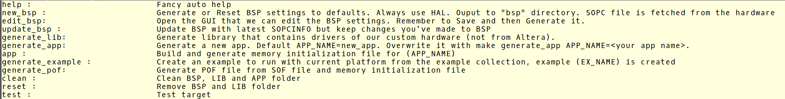
There are five steps:
- Create a board support package (BSP) for the CPU
- Generate a library
- Prepare your source code, or use an example
- Generate an application
- Create a POF file
The POF file is exactly what the Intel programming software takes to burn the nonvolatile configuration memory on the board. If you’ve done the getting started tutorial, you should know how to burn this file into the FPGA.
There’s more detail on the blog, but here’s the basic command lines for the example frequency counter, all issued from the sw/recon_0 directory:
# step 1
make new_bsp
# step 2
make generate_lib
# step 3
make generate_example
# step 4
make app APP_NAME=frequency_counter
# step 5
make pof APP_NAME=frequency_counter BOARD_NAME=max1000
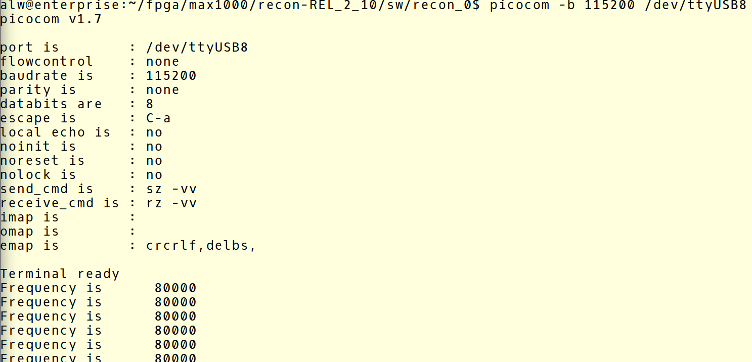
Once you program the FPGA, you should see a USB serial port enumerate. Use a terminal program set to 115,200 baud and you’ll see the software counting an internal clock.
Software Things
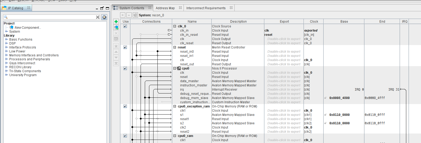
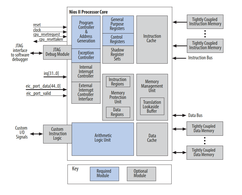 The NIOS II is a pretty robust CPU with a good C compiler implementation. Check out the component block diagram to get an idea of how things are laid out. However, since you’ll mostly be programming it in C, you probably don’t care much about the actual layout, but more the board support package (BSP) and associated libraries.
What does the software look like? Good question. There are two files. One is just a little Arduino-like main:
#include <system.h>
#include <sys/alt_sys_init.h>
#include <sys/alt_irq.h>

void setup();
void loop();

int main(void)
{
/* Altera sepcific */
   alt_irq_init(0);
   alt_sys_init();

   setup();

   while(1)
     {
     loop();
     }
}
The main code is a little longer but shows how the libraries are set up very similar to an Arduino. Here are a few lines:
/////////////////////////////////////////////////////////////////////////////////////////////////
// Bind Serial Object to UART_0 component by assigning the base address
Serial.bind(UART_0_BASE);

/////////////////////////////////////////////////////////////////////////////////////////////////
// Setup serial object with baudrate 115200
Serial.begin(115200);

/////////////////////////////////////////////////////////////////////////////////////////////////
// Setup mode of Pins, we have INPUT, OUTPUT and OUTPWM modes
pinMode(0,OUTPUT);
pinMode(PWM_PIN,OUTPWM);
setPWMPeriod(1000);
analogWrite(PWM_PIN, 200);

. . .

/*
* ISR that handles IO IRQ
*/
void io_isr(void* freqCntr)
{
///////////////////////////////////////////////
//Read back which pin is interrupted
   u32 pin = recon_io_rd32(IRQ_STATUS);
///////////////////////////////////////////////
//Clear Interrupt
   recon_io_wr32(IRQ_STATUS,pin);
///////////////////////////////////////////////
// On each interrupt, we increment the counter
   (*((u32*)freqCntr))++;
}
Next Step
Not bad for a few quick command lines. Of course, the real test is when you go to make customizations, but this should give you an excellent start. If you look at the cmn (common) subdirectories in the hw and sw directories, you can see how the existing I/O devices are created and controlled. That should get you started pretty easily. There is a standard called Avalon for how things should interface with the NIOS core. The example I/O devices use the simplest method, but there are more complex setups like memory mapping if you need it.
You can send the Makefile the edit_bsp command if you want to experiment with changing the board support package. You’ll need to do a little research, though, as there are lots of options.
In addition, regenerating the NIOS II core isn’t trivial although the Quartus project files are in the hw subfolder. In particular, we had to take the following steps to get everything upgrading and building properly:
- Open the recon_0.qpf file in Quartus
- Open the recon_0.qsys file which opens Platform Designer
- Go to Tools | Options in Platform Designer
- Set the IP Search Path to the hw/cmn directory
- Save your work in Platform Designer
- Go back to Quartus and compile your design
- Copy the .sof file generated from the output_files directory to the release directory (you might want to backup the old sof file, first)
Just make sure you pick up the right pof file from the sw directory after you go through the five steps to build your app and not the pof of the blank CPU in the hw directory. Don’t ask us how we know that.
You should only have to set the directory one time. Of course, there are lots of tempting things to play with in the Platform Designer, too, including adding custom opcodes to NIOS.
If you prefer the GUI method or you start working with the tools to do your own extensions, you can follow the official tutorial. You might also find the official page useful. There’s also a video, that you can see below.
If you need more of a jump start on FPGA coding, check out our FPGA boot camp over on Hackaday.io. It doesn’t use the MAX10 part, but the general principles still apply and the tutorial is hardware-neutral until the last boot camp, anyway. If you are interested in using the MAX10 analog inputs, the same site has a recon_0 setup for that, too.


“Ok, we’ll admit it. We like FPGAs because it reminds us of wiring up a 100-in-1 kit when we were kids.” Hey! What about those who never were kids? Seriously, there’s still the disconnect between the physicality of the latter and the mental breadboard of the former.
Oops, sorry Ostracus; my fat finger hit ‘report.’ Sorry
I thought the problem with Nios was that the license is a little pricey for the average maker?
Historically, NIOS II/e (economy edition) was free, but looking just now I couldn’t find anything current that specifically says that: https://www.intel.com/content/www/us/en/products/programmable/processor/nios-ii.html
Ah, ok if you dig around there you’ll find:
Nios® II/e “Economy”
Intel specifically designed the Nios® II/e “economy” processor cores to use the fewest FPGA logic and memory resources.It is now offered free for both Nios® II Classic and Nios® II Gen2 processors. No license is required with the Intel Quartus® Prime software and Intel Quartus® development software version 9.1 and later. The Nios® II/e core has higher performance but is in the same cost class as a typical 8051 architecture, achieving over 30 DMIPS at up to 200 MHz. It is using fewer than 700 logic elements (LEs).
The core is supported by the Nios® II Embedded Design Suite (EDS), including the Eclipse-based Nios® II Integrated Development Environment (IDE).
The free Nios® II/e core features:
Up to 2 GB of external address space
JTAG debug module
Complete processors in fewer than 700 LEs
Optional debug enhancements
Up to 256 custom instructions
I remember that the free version of NIOS used to only work on the hook. Am I mistaken, can it be used completely freely, without jtag cable attached?
700 LE sounds very compact. I considered ZPU for my current project, but gave up figuring out their mess of weird and incompatible implementations. Ended up using a 6502 core.
Nios-e is completely free. I used it in my master thesis and it worked just fine.
The other Nios variants need a license or the JTAG cable to be connected.
Another project in this space is LiteX (https://github.com/enjoy-digital/litex). It supports a few different open source soft cores and has a ready library of peripherals. There’s a getting started demo that goes through creating a design and booting Linux on it.
no hook. Honestly. The /e version is free and works standalone. And it is small.
I am still confused what is a difference between MAX 10 and Cyclone 10 LP, there is MAX1000 board and CYC1000, they are very similar, Arrow has MAX 1000 with 8k lUTs foer $30 and CYC1000 with 25kLUTs for $40, which fpga family is faster?