A few years back, a company by the name of Pano Logic launched a line of FPGA-based thin clients. Sadly, the market didn’t eventuate, and the majority of this stock ended up on eBay, to eventually be snapped up by eager hackers. [Tom] is one of those very hackers, and decided to try some raytracing experiments with the hardware.
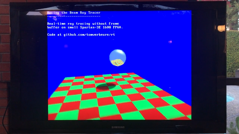
[Tom] has one of the earlier Pano Logic clients, with VGA output and a Xilinx Spartan-3E 1600 FPGA under the hood. Due to limited RAM in the FPGA, and wanting to avoid coding a custom DRAM controller for the memory on the board, there just wasn’t room for a framebuffer. Instead, it was decided that the raytracer would instead “race the beam” – calculating each pixel on the fly, beating the monitor’s refresh rate.
This approach means that resource management is key, and [Tom] notes that even seemingly minor changes to the raytracing environment require inordinately large increases in calculation. Simply adding a shadow and directional light increased core logic utilisation from 66% to 92%!
While the project may not be scalable, [Tom] was able to implement the classic reflective sphere, which bounces upon a checkered plane and even added some camera motion to liven things up through an onboard CPU core. It’s a real nuts-and-bolts walkthrough of how to work with limited resources on an FPGA platform. Code is available on Github if you fancy taking a further peek under the hood.
If you’re new to FPGAs yourself, why not check out our FPGA bootcamp?


An FPGA-based thin client? Why? I I’m having trouble understanding why that would be advantageous for a thin client versus just using an embedded CPU.
Back in the day, the thinking was: no software, no viruses, centralized update management.
This was right before Intel launched the Atom.
Bad idea or not; today they are fantastic toys for FPGA loving hobbyists!
Seems ridiculous, though. You still write “code” for the FPGA, and it can have bugs too.
They did go out of business. :-)
A lot less “code” though. And, I don’t know this for a fact but it seems likely, I would think errors in an FPGA “hardware” design would show up immediately, rather than potentially hiding for years until some particular combination of circumstances arose.
Maybe there was a soft CPU in the design where appropriate.
Still yeah it does seem like a bad idea, CPUs are surely always cheaper. FPGAs do well in specific tasks that can be coded for, where the tradition “in -> execute -> out” serial method used by CPUs isn’t suitable. Weren’t ARM chips with onboard display controllers etc available back when this was made? Even if they weren’t, surely a set of chips was. You could get graphics cards fairly cheap in the 1990s. Even the cheap ones had onboard processors for basic acceleration. Glue one of those to an Ethernet card and you’re more or less there.
Late 1990s is when the “thin client” fad was about, IIRC. The invention of Java and some amazing hype drove it. When is this gadget actually from?
Oh OK, answer my own question, Pano Logic was only founded in 2007. So they’re really going for a new paradigm with the no-cpu. Maybe victims of some of the hype FPGAs have received, although that’s mostly been limited to geeks who know what one is.
Such is the demoscene. You do these things not because they are easy or practical, but because they are hard.
TO THE MOON!
And the other things!
For those who are interested in Pano Logic boxes, you can the low level details here: https://github.com/tomverbeure/panologic
The Spartan-3E 1600 is already decent sized. The Pano Logic G2 FPGA is a Spartan-6 LX150 and huge. Getting an image going on that one is an on-going project, but it’s close and a matter of days. Info is here: https://github.com/tomverbeure/panologic-g2
Both Panos can be bought for a handful of dollars on eBay. There is no better value when it comes to complete FPGA boards for hobbyists.
Thanks for sharing your work, I have been wanting to dive into reverse engineering both the G1 (I have a few of them already) and the G2 and now that the ISE 14.7 supports the LX150, thats really great news – I did not know this until I read your article.
Unfortunately, most of the ebay sellers charge an arm and a leg for postage to europe so I have yet to get a cheap deal on a few G2s. My plan with these boxes was to use them for hardware emulation of old game consoles/vintage computers and other experiments where a large FPGA is useful.
Send me an email at hombre at gmail. I might be able to get you a G2.
There are a lot of things that are best NOT done with software…
Very, very cool. Thanks for sharing the code!
Pulled the trigger on a cheap NIB eBay deal. Guess this is as good a time as any to dip my toes in to FPGAs. Looking forward to playing around with this hardware.
Careful, most that I can see on Ebay are second gen ones which means an FPGA with no free tools unfortunately.
This is not true anymore!
The free Win10 version of ISE 14.7 supports the LX150 without limitations. I’ll be writing up instructions on that soon.
Awesome! Thanks for that. I might get one to play with. Are VGA and DVI/HDMI mutually exclusive?
There are 2 outputs, each with their own Chrontel video chip: DVI and micro-HDMI.
In addition, the DVI connector has the analog VGA pins wired up. According to the Chrontel spec, you can’t do both VGA and DVI, but I’m not entirely sure.
So you could do: DVI+HDMI or VGA+HDMI.
But since HDMI is a superset of DVI, you could connect a DVI cable to the HDMI and you’d have VGA+DVI.
HA, and I had bought a ton of the G1 hardware :D for peanuts.
/me has like 50 of them I was thinking maybe a beowulf cluster or perhaps updating the plan9 sparc port and having a ton of little sparcstations inter networked running plan9 using the temlib project for the sparcstation core.
I have about 20 G1s and 25 G2s (which I bought thinking they were G1s, before I knew they were now usable with the free ISE version.)
Also thinking hard about how to use them in a cluster.
How easy would it be to hack that to run on Linux? I’m under the impression that since it’s apparently a Linux VM, it would be reasonably easy to just run the VM on another Linux. Maybe it can be possible to run the ISE without the VM?
I have it running on a Linux in a Linux VM.
And others have just reported that they were even able to run it on Linux native by hacking the Ethernet MAC.
This is all bleeding edge at the moment. I’ll write down my findings.
But to run it under Linux in a Linux VM, I used “virtual applicance export” on Win10 and then import on Linux.
See here:
https://twitter.com/udifink/status/1071030126337581058?s=21
If I already have the free ISE 14.7 installed on Linux, would it be possible to just extract the license from the VM and apply it to the already installed ISE?
It seems that it’s possible to copy the support for the larger Spartan 6 devices from the VM to a standard installation of ISE14.7. (I’ve already got ISE installed on Windows 10 for playing with Coolrunner. Then there’s Vivado. So many GB of Xilinx software!)
It’s not a licence that you have to copy but the contents of the 14.7/ISE_DS/ISE/spartan6 folder. Once you’ve done this, ISE knows about the larger devices. You may need to copy a similar folder for PlanAhead. I’ve ordered some G2s but not got them yet, so can’t be sure.
Damn. It seems to do need a license otherwise it fails later when mapping the design. Sorry.
…unless you change your MAC address. :-)
It’s actually very easy, but takes forever due to the file sizes involved. Basically:
1. Install the older webpack release on Linux and license it in the usual way.
2. Rename /opt/Xilinx/14.7/ISE_DS to /opt/Xilinx/14.7/ISE_DS.spartan3
2. Download and unzip the new webpack release.
3. Import the .ova file into a VM (I used virtualbox).
4. Copy /opt/Xilinx/14.7/ISE_DS from the VM to /opt/Xilinx/14.7/ISE_DS.spartan6 on the “real” machine.
5. Create a syn link from /opt/Xilinx/14.7/ISE_DS.spartan6 to /opt/Xilinx/14.7/ISE_DS
That’s it. To switch back to the older version for other devices just delete the symbolic link and create a new one from /opt/Xilinx/14.7/ISE_DS.spartan3.
Well this is amazing. Thanks for making a nice writeup too, instead of a long bla bla bla video.
Wow! Just bought 15 units for $58 shipped. Now that ARM opened the soft IP for Cortex-M3 it should provide a fun platform to play with. Especially if we can get DDR3 and ethernet working.
Ultimately, I want to use these things as a console. That’s a matter of getting a USB stack up and running for controls.
Wrong reply. :-)
“Now that ARM opened the soft IP for Cortex-M3”
I understand that Xilinx only supports that on 7-Series and later using their Vivado toolset (i.e. not on this FPGA without a lot of work).
Bummer if this is the case… Can anyone with Vivado installed verify whether you can or cannot instantiate an M3 core on a Spartan-3E? I’ll send you a free thin client ;)
To answer my own question Vivado only supports 7-series+ processors…
Thanks Allan, you indeed were correct. I did find the Arty A7-35 from digilent which should support the new Cortex-M soft cores. Not a bad value for $119. Just trying to get my head around the Vivado licensing now…
How about converting one into a 2600 console?
mately, I want to use these things as a console. That’s a matter of getting a USB stack up and running for controls.
Could https://github.com/emard/fpga-usbhid-host be adapted to use ulpi interface? Seems quite a simple solution if you know exactly what controllers you want to support.
I think something like this could be a solution.
Though I was more looking at adding a small RISC-V CPU and going the SW route. It’s much easier that way to iterate on bugs.
DVI and VGA connectors will both have an I2C host in them. Bit hacky, but between them you should have enough I/O for a SNES controller at least. Or better would be use an I2C GPIO expander like SC16IS750 which would also give a serial port too.
That’s very hacky indeed. But it should work. I love it! :-)
Ok. I bought two of these from eBay; one with DVI one with VGA. I’ve been meaning to get into FPGA stuff for a while.
“JVisitor” said he has posted schematics to dropbox (https://hackaday.com/2013/01/11/ask-hackaday-we-might-have-some-fpgas-to-hack/#comment-4617867), but alas the link is dead. If someone downloaded the docs back in June could they please make them available again? I just bought 3 VGA and 3 DVI versions for myself for Christmas on ebay so they are still available.
Replying to my own reply.. JVisitor has made the schematic (and gerber files) available again! Looks like you can put your ohm meter away for a while TomV.
Wow!
At first I was skeptical… what’s the point of an FPGA “dev-board” without any GPIOs and limited in peripherals to those available in most any SBC?
But this seems to be some incredible work in pushing the limits of parallel-execution that I’d almost forgotten also makes FPGAs what they are. Nicely-done.
And then, I came across this!
http://blog.2gn.com/wp-content/uploads/2013/07/IMG_006.jpg
Is this the case with all the models?
Now… how to tap into them vias without a ratsnest…
hrm… dud-link…
http://blog.2gn.com/electronics/in-search-of-fpgas-or-pano-logic-generation-1-teardown/
Last picture, there.
Incredible work by both you and The Cranky Sysadmin!
The link that you posted is broken, but I think you meant to link to 0086.jpg instead of 006.jpg.
The rats nest of vias are a feature: they may it so much easier to measure things on a live board with an oscilloscope board! With a steady hand and microscope, you should be able to solder some thin wire-warp wires on them as well.
That said, I really like the suggestion made by “nes” about connecting an I2C to parallel chip to the DDC/CI pins (which carry regular I2C) of the DVI or VGA connector.
Wii Classic controller is already I2C actually. I apart from the power supply I _think_ you could almost just chop it’s connector and replace with a VGA plug. However it wants 3.3V and VGA/DIV/HDMI provides 5V so you’d want some sort of regulator in line. https://wiibrew.org/wiki/Wiimote/Extension_Controllers/Classic_Controller
Nice board to play around with (especially the LX150 part on the G2), but paying $50 shipping to send it to the Netherlands is a deal breaker :'(
Send me an email to hombre at gmail.
Thanks guys 12 bucks and I don’t even know how to FPGA. At least it looks pretty
I got my (used) DVI thin client yesterday, but I still don’t have a XILINX JTAG cable and I can’t figure out if it is even working. When I plug in a power supply and an Ethernet cable the light starts blinking and after a while it is solid orange, but there is no signal on the DVI port. Is that normal? Does the video turn on after connecting to a “server” or something?
And another question for the XILINX gurus (I play with Altera parts mostly) – I have an Avnet Spartan-6 micro board and a Digilent Nexys 2 (Spartan 3e) with built-in USB-JTAG adapters. Is there any way of using them as JTAG adapters for other boards. Thanks.
It’s normal that you don’t get an image: I don’t get one either after bootup, and that’s true for both the VGA and the DVI version.
I will add bitstream file to the “blink” example of my panologic-g2 github repo so you can quickly test if everything is working, once you’re able to connect JTAG.
I’ve only used a clone of the Digilent Xilinx JTAG programmer (~$22 on AliExpress), but others have been able to make it work in different ways to load data into a Xilinx FPGA. For example, the xvcpi project (Xilinx Virtual Cable for Raspberry Pi.)
One day, I’ll get around to trying that as well.
Thank you for answering my questions.
I have been working on the pano G2 DVI client. You can see some of my results here: http://daveland.us/pano-logic-g2-reverse-engineering/
In short I can now see the xc6slx150 in impact on an older version of ISE. Still need to get the VM version that I can complie and map to talk with my pltform cable. I hope to have a Hello world light flashing on the G2 client before xmas
dave
Great thread. Can someone help to share how configure the SPI flash found on G1 and G2 in iMPACT?
Here it is: The Spartan3 G1 flash density is 8M and M25P80 from the dropdown in iMPACT.
On the Spartan6 LX100 or LX150, the density is 128M and M25P128 in the dropdown.
First, “Create a PROM File”, in iMPACT. It will take the flash density. Assign it to Rev0, add the bitstream file. The hit “Generate File”, to create the .mcs file.
On the boundary scan, right-click the dotted box indicating the flash ROM, and assign the .mcs file. Now the flash chip turns green and will have “program” in the right-click context.
I’m having a problem reading/erasing/programming G2 with the LX100, the JTAG Vref drops in the middle of the operation and programming fails. Anyone else has this?