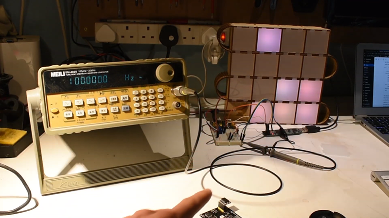
[John] wanted a project to help him learn more about FPGAs. So he started with his wooden clock — made with an Arduino — and ported it over to a Lattice FPGA using Icestorm. What’s nice is that he takes you through the steps he used to simulate the design using the Falsted simulator and then realizing it in the FPGA. Since he’s just starting out, it is a good bet he ran into the same rough edges you will (or did) and sometimes that can really help get you over the hump. You can see a video below, and the code for the project is on GitHub.
For example, after mocking up a circuit design in Falstad he realized he could make one large counter instead of several modules, and he contrasts that to a more modular approach. He also ran into a feature that was simple for the Arduino but difficult for the FPGA. He got it working, but it took some optimization effort to make everything fit in the relatively small FPGA he was using.
The original motivation for [John] was seeing how [Mattvenn] created a custom peripheral for the RISC-V CPU. In that case, you have a whole CPU at your disposal, but we agree that it was wise not to start with that as a first project.
We also liked the approach of thinking about the logic first and then moving on to the Verilog. Granted, if you have a lot of experience it is customary to skip that step and just visualize your desired logic in Verilog, but that comes with experience.
We’ve written a lot about the Icestorm project in the past, including our own getting started tutorials. But sometimes having a choice of examples and starter projects can make things easier.


Falster/Falstad (Spelling)
Instead of “if (count[3] & count[0]) begin // 9”, it’s easier to just write “if (d0 == 9)”
Also I wouldn’t use 4 modules, nor one long counter, but 4 smaller counters:
reg [3:0] d0;
reg [2:0] d1;
and then you can do d1 <= d1 + 1
The module does account for smaller counters: https://github.com/tuna-f1sh/wooden-bits-fpga/blob/master/counter.v#L8 . I kept them all 4 bits however, for ease of displaying on my square matrix clock design. If I’m not mistaken, you still need to have a modulo reset for a BCD clock 3/2 bit counter otherwise it would count to 7/3.
The reason for bit logic rather than compare was that I read somewhere that it offers some optimisation, as it will not create a gate comparing all bits, just the bits that need to be read. The otimisation may happen at synthesis but worth being clear!
I was referring to the long counter here: https://github.com/tuna-f1sh/wooden-bits-fpga/blob/master/binary_clock.v instead of writing count[6:4] <= count[6:4] + 1, I would put those bits in reg d0/d1/d2/d3, and then do: d1 <= d1 + 1, and d1 <= 0, and d2 <= d2 + 1. Easier to read than count[12:11] The reason for bit logic rather than compare was that I read somewhere that it offers some optimisation,
True, but difference on an FPGA is minimal, and the tools may even be smart enough to do the optimization for you. It’s better to focus on readability, and optimize only when you don’t meet the area/timing constraints.
Thanks for sharing Al. Your getting started tutourials were the main reference during my learning.
What multimeter is in that shot?