In recent months, the ability to hide components inside a circuit board has become an item of interest. We could trace this to the burgeoning badgelife movement, where engineers create beautiful works of electronic art. We can also attribute this interest to Bloomberg’s Big Hack, where Jordan Robertson and Michael Riley asserted Apple was the target of Chinese spying using components embedded inside a motherboard. The Big Hack story had legs, but so far no evidence of this hack’s existence has come to light, and the companies and governments involved have all issued denials that anything like this exists.
That said, embedding components inside a PCB is an interesting topic of discussion, and thanks to the dropping prices of PCB fabrication (this entire project cost $15 for the circuit boards), it’s now possible for hobbyists to experiment with the technique.
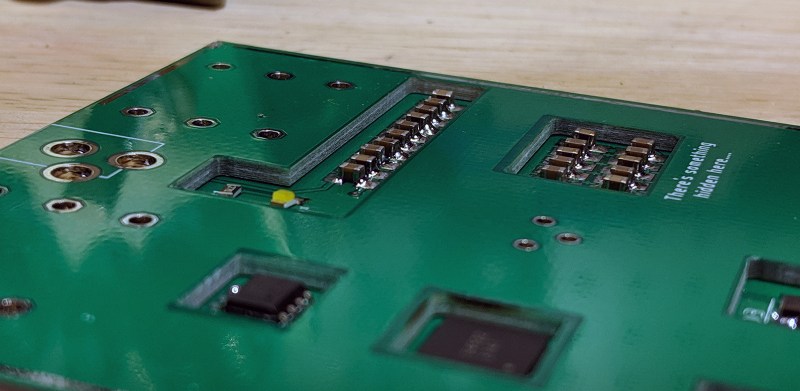
But first, it’s important to define what ‘stuffing components inside a piece of fiberglass’ is actually called. My research keeps coming back to the term ’embedded components’ which is utterly ungooglable, and a truly terrible name because ’embedded’ means something else entirely. You cannot call a PCB fabrication technique ’embedded components’ and expect people to find it on the Internet. For lack of a better term, I’m calling this ‘Oreo construction’, because of my predilection towards ‘stuf’, and because it needs to be called something. We’re all calling it ‘Oreo construction’ now, because the stuf is in the middle. This is how you do it with standard PCB design tools and cheap Chinese board houses.
Previous work
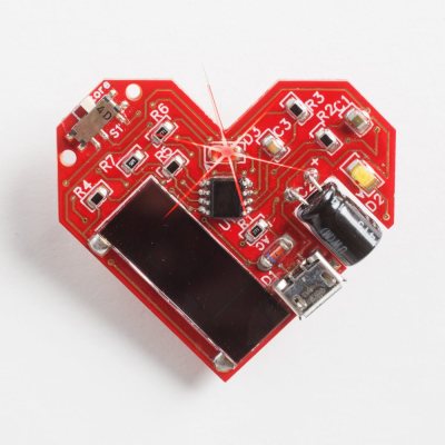
The immediate inspiration for this build comes from designer2k2 and a flat-pack Christmas ornament. This project used castellated pins and a series of holes to mount SMD parts to the side of a PCB instead of the top or bottom. While soldering electronic components to the side of a PCB is somewhat novel, mounting electronic components to the side of a PCB is nothing new. Lumen Electronic Jewelry is producing a PCB ‘heart’ pin (right) with a capacitor and USB port mounted inside a cutout in the milling layer of a PCB. Likewise, other PCB projects — mostly PCB business cards — have experimented with mounting other components in a cutout in the milling layer. I have seen coin cell battery holders that use PCB cutouts with two ‘tabs’ that capture a battery between fiberglass.
The idea of embedding components within a stack of fiberglass and copper is something we really haven’t seen before in the small-scale hobbyist world, but it can be done. Embedded components — there’s that ungooglable term again — can be done in very expensive products. The reasons for doing this range from saving physical space, better EMI shielding, and making something more difficult to reverse engineer. This is a technique for military and aerospace components, where price is no object.
Boards for military and aerospace work are one thing, but the past year saw a significant amount of discussion over embedded components, albeit for all the wrong reasons. Bloomberg’s Big Hack was a story about Supermicro motherboards shipped to Apple and Amazon that had additional components giving Chinese hackers a back door. This story was widely criticized, Apple and Amazon have fervently denied having found compromised motherboards, and any day now I’m expecting Supermicro to file suit in a libel case. This story did however generate a lot of discussion over how such a hack could happen. The top minds of the Twitterverse believe this could be done by embedding a small microcontroller inside the motherboard’s PCB, between the baseboard management controller and its Flash memory. This small microcontroller stuck between a few layers of PCB could in theory change a few bits of the BMC’s Flash to give attackers a back door, and Trammel Hudson gave an interesting talk at CCC discussing the theory of this fictional hack’s operation. It’s within the realm of possibility, but the smart money says this didn’t happen with Supermicro motherboards shipped to Amazon or Google. In any event, x-ray inspection or even a flying probe test would reveal any ’embedded component’ was in the PCB.
Layering Printed Circuit Board
For this build, I have extended these techniques slightly by mechanically bonding the layers of PCBs together with solder. This was previously done by Voja Antonic and his work in building enclosures out of FR4. His approach was to create a strip of bare copper around the perimeter of each side of the enclosure. By mounting these sides of the enclosure at the correct angle, soldering the two flat planes of PCBs into a three dimensional shape is as simple as running a soldering iron over the exposed copper on the perimeter.
Each PCB in the stackup has exposed copper along the perimeter. By applying solder paste and clamping the boards together they’re read for reflow.
I used Kapton tape as the clamping method since it will have no problem holding up to the heat of the oven. After baking it, sandpaper is all you need to clean up the edges.
This circuit
The circuit for this build is a guitar pedal. More specifically, it’s a slight modification of a Dallas Rangemaster, with the actual schematic borrowed from Fuzz Central (the RangeBlaster). There are several reasons for demonstrating this PCB technique in the form of a guitar pedal, and for using a Rangemaster circuit in particular.
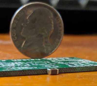
The Rangemaster circuit in particular was chosen because it is a very simple circuit. It’s only a single germanium transistor and a handful of resistors and caps. My choice of putting a Rangemaster circuit inside a PCB is driven simply by component count; it is the simplest circuit that does something. As for demonstrating this technique in a guitar pedal, I have far more sinister reasons. The market for guitar pedals makes even less sense than the audiophile market. If you come up with a circuit and coat it in epoxy, you’ve just made a thousand dollar pedal. No, that is not a joke. I am simply capitalizing on the gullibility of consumers with an interesting fabrication process.
The basis of the circuit is exactly what you would expect for a guitar pedal: there is a 3PDT footswitch, a pair of 1/4″ jacks, a 2.1mm DC jack (center negative, because Boss), and a standard PCB mount pot 10k, audio taper. The active part of the circuit is a vintage OC44 transistor in a TO-5 package. These are the only components visible on the finished PCB.
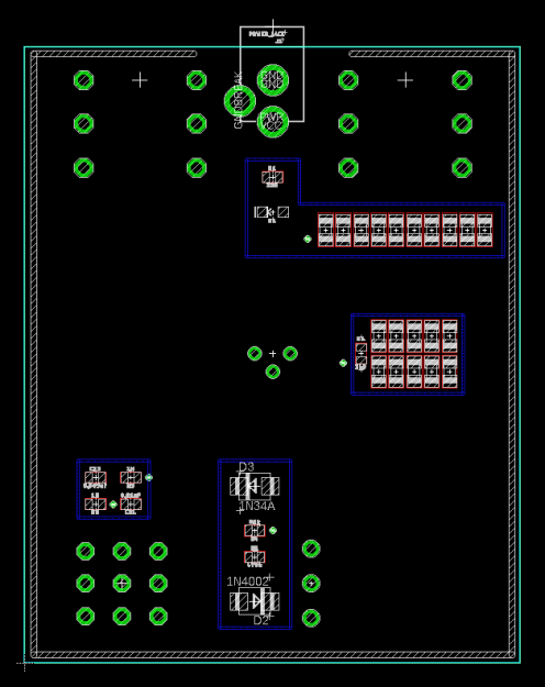
This circuit board was first constructed by laying out the through hole components in logical places, then dropping the surface mount components in places that made sense. Again, this is an exceedingly simple circuit with less than a dozen parts, in the schematic. Once that was done, it was only a matter of copying the PCB to a new file and adding cutouts around the parts. This board was done in Eagle, giving me the ability to add many layers to the board which could then be added to the CAM manager to create the Gerbers.
The real ‘trick’ with this technique is encapsulating components within a PCB stackup. While this can be done with a standard PCB thickness of 1.6mm per layer (three layers are required for complete encapsulation, resulting in a final thickness of 4.8mm), I used 0.6mm thick PCBs for the top and bottom layers. This resulted in a final thickness of 2.8mm. This is thin enough that the assembled piece does not register in your mind as a stack of PCBs. It’s thin enough that one could easily believe this is just a normal PCB.
It’s easy to create a PCB, and if you know what your board house can do, it’s easy to create internal cutouts on a board. There is absolutely nothing new about the previous thousand words. The trick to Oreo construction is mechanically bonding the layers together. This could be done with glues and resins, but taking a page from Voja’s work, I decided to use solder to attach one layer of PCB to another. This was done by a copper trace around the perimeter, disconnected from any ground planes or pours.
The assembly process is as simple as populating and soldering the bottom layer board with surface mount components, preferably with lead free solder paste. Then, leaded solder paste is applied to the perimeter traces, the boards are clamped together, and the entire assembly is thrown into the reflow oven. After that, it’s simply a matter of populating the through hole components.
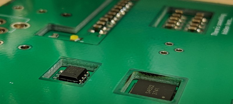
There are other ideas I considered to connect these different PCBs together. I could ‘stitch’ them together with vias and through holes, using small bits of wire to both align and mechanically attach each layer together with solder.
Limitations of this technique and areas of further study
While you can embed capacitors, resistors, and microcontrollers inside a stack of PCB, there are limitations. First and foremost, the Rangemaster clone circuit calls for 47 μF capacitors. This value is much too large for small SMD caps, and the (physically) smallest caps I can find with this value are on the order of 10mm thick. Unless you want a circuit board that’s half an inch thick, these caps are far too large. The workaround for this problem is to add many caps in parallel.
This leads to another problem. The original circuit used electrolytic capacitors, not small ceramic capacitors. Because I’m using arrays of ceramic caps, the actual capacitance is less than the sum of all the capacitance in the array. MLCC capacitors should be derated when biased (as they are when using them as a bypass cap), and the capacitor I ‘constructed’ does not have the correct value in the circuit. Yes, the capacitance of ceramic capacitors is dependent on their voltage, but you can aaay yolo around this by simply adding even more capacitors.

Additionally, no project that uses this technique will be able to use large parts. If you have a project with a small boost power supply, you probably have a relatively large inductor. Inductors of a sufficient rating for a beefy power supply will be too tall to embed into a single layer of FR4. The same is true for components handling high power, as they’re usually physically large and must dissipate heat, the latter being a problem for a component that is effectively trapped inside a fiberglass box.
Despite the problems, this is an interesting technique of PCB fabrication. Combined with the dropping prices of custom-made PCBs — the boards for this entire project cost less than $15 USD total — I would expect to see many PCB artisans picking up this technique.
This project was just a demonstration of what is possible with Oreo construction, but given the huge advancements in artistic PCBs, this is in no way the limit of what is possible. Given we’re now in the golden age of reverse-mount LEDs, it’s possible to encapsulate the driver and the LEDs of a gigantic matrix inside fiberglass. With Oreo construction, an entire PCB could be just a brick of fiberglass when it’s off, and a glowing rectangle when it’s on.
If you’re wondering what this Oreo construction guitar pedal sounds like, well, it’s a Rangemaster treble booster. Brian May’s guitar work for Queen would be the most popular example, but Brian May is a little too unique to really get a sense of what this sounds like. A better example would be Tony Iommi of Black Sabbath, something from the first two Zeppelin albums, or Clapton on the Blues Breakers album. That’s a lot of sonic territory, but this is a better demo of a Rangemaster than anything I could produce. In any event, but the entire idea behind this was to build the simplest circuit possible inside a PCB, not to do anything fancy. A Rangemaster is one transistor, so that’s what I built.






See: cordwood modules – https://archive.computerhistory.org/resources/physical-object/control_data_corporation_cdc/X402-84A.lg.jpg
So oreo construction could also be called thin cordwood?
What about using oreo construction to make the halves of cordwood modules?
Mind. Blown.
Compacted cordwood? High density cordwood? Or maybe cordwood is LDO (low density Oreo)?
Plywood ?
The picture is quite small but it seems like there is principal(?) difference between cordwood and oreo construction:
In cwc many components are connected between the two layers (one end of any two-pin component connected to the upper- and the other to the lower layer), while that seems quite useless/impractical/difficult/impossible with oreo construction and smd components.
But exactly that construction technique seems like the major idea behind cwc (cordwoodconstruction)…
See also this 7 segment display made up of multiple layers of PCB stacked.
https://hackaday.com/2016/08/23/charliplexed-7-segment-display-takes-advantage-of-pcb-manufacturers/
Why the two different solder pastes (lead-free inside and leaded to close the “cookie”)?
Leaded solder paste has a lower melting point. The idea being to solder the parts on with lead-free, then close the cookie with leaded paste, which can be run at a lower temperature, thus not melting the already soldered-on parts!
That makes sense. If this is the case, choose SAC lead-free solder (217 C) rather than the bismuth variety that’s been gaining popularity (138 C). The latter melts at a *lower* temperature than 63/37 leaded (183 C).
The point of using lead is that low melting lead-free alloys tend to have otherwise unwanted properties such as growing tin whiskers or being susceptible to tin pest, or not melting/solidifying completely over a narrow range of temperatures but instead turning into “porridge” in the middle.
It’s a much more delicate business to choose the right solder when you’re not allowed to use lead or other dangerous but useful substances like cadmium.
Seeing that you can do lead free on both sides of a PCB through a reflow oven this doesn’t really stack up. You could easily reflow the parts on the board with lead free then close the cookie with lead free. This is already similar to SMT RF Cans on PCBs.
I thought the same, but maybe it is faster to reflow since the heat would need to penetrate a board’s thickness.
You can also use good leaded solder for both tasks.
I like this. I’m using a variation of it for a project I will kickstart soon: I use the battey pack as one side of the “oreo” and components on the top don’t expose their connections. Except for a nano which I melt plastic over. (I made a video, if you’re interested on YouTube).
I’m not sure what to make of this.
Seeing a hacker attempt some new challenge and conquer it is a great thing. It certainly cannot hurt to stretch one’s abilities and try something new. Maybe we should all try to build one board like this at some point in our hacking hobbies.
But.. it also kind of makes me think that it is a sign of taking all that is wrong with the commercial hardware world and transplanting it into the hobbyist one. Something I think we as a society need is more devices with visible internals, not better covered up ones. Soldered together component/pcb sandwiches are naturally going to be hard to hack, hard to repair and hard to learn from.
As a kid I was fascinated with antiques. I especially loved looking at all the machines at the Henry Ford Museum. This wasn’t because I had any sort of retro-nostalgia and certainly not because I wanted to live in any less-advanced times. Quite the contrary, I wanted to grow up to build new and better things myself. I was inspired by all this old stuff precisely because it wasn’t covered up. One could easily see all the gears, rods, belts and pulleys. One could easily work out in one’s head a great deal about how these things operated.
I will always remember the first time I saw someone take the case off of a modern clothes washer. I was very surprised to see that inside it looked so similar to the antiques I had seen in the museum. Modern washing machines weren’t some totally new, unrelated design to the old ones. They are just covered up with big metal boxes that don’t really have anything to do with washing clothes. That is a great summary of how most modern consumer technology is and it is very uninspiring. We can’t have next-generation technology if the next generation has no engineers!
Well, anyway.. one board of hidden components here and there isn’t going to destroy the engineering minds of a generation. I just hope that this idea remains a technique that is only occasionally used just to show that one can and does not become a new common standard in hobbyist development.
Nah, it just about making a cheaper, product using a pcb as a chassis (chassis are expensive).
You can use 2 aligned visas and a soldered wire to make it stick together and still hackable.
Here’s a hack:
Just solder the wire to one side of the cookie and bend it over on the other side. Even easier to disassemble! But maybe not as strong. Use 4!
Just stitch them with wire the way sometimes leather is stitched…
+1 for pointing out that it is fundamentally about using pcb to build a cheap chassis.
My suggestion for joining them togehter is to take a technique used for layered perspex containers and bolt the PCBs together.
– Using a small countersunk bolt would mean that side of the pcb stack is flush
– You would need to find something suitable to use for the nut. Perhaps a nylon nut that also worked as feet for the pcb container?. I imagine that press-fit nuts probably exist that would allow the nut side of the pcb stack to be flush, or nearly so.
– When you want to hack or repair the circuti you just undo the bolts
Something I think we need is a society is just the ability to appreciate someone’s project without deciding we think it represents toxic design philosophy
It’s not as bad as opening up something only to discover a solid potted block of epoxy.
Did you not hack together an X-Ray device yet? You can make the tube yourself. Really. :)
https://www.youtube.com/watch?v=-0G4-JicCIw
This is all fun for a while for hobbyists until they realize it’s difficult to repair or modify. It may be fun for making badges… for a while and then people will dislike them when the hype is over.
Regarding commercial applications, I doubt this will be effective. The extra effort it takes to produce all devices you make to prevent it from being reverse engineered, does not relate to the effort of reverse engineering a single device. So in short, it will drive up production costs but doesn’t solve the copy problem. It’s basically the same as potting or grinding down the component values/numbers.
The only true reason for this technique should be to shield signals or to increase the component count without the PCB getting larger in X or Y. And in some very rare cases the PCBs could be layered so many times that it forms a case. But I wonder if a case made of PCB material is really prettier/more practical then a 3D printed one. They both have their disadvantages over a decent case or a simple project box.
But from a purely technical tinkering point of view… this is fun!
I like being able to make the smallest and densest boards possible so that I can embed in something else without affecting aesthetics. This is definitely relevant to my interests. It’s definitely not an every day technique, but it offers a lot of size flexibility.
I totally agree with repair difficulty going up. I was going to make a joke about it ruling out Keeley mods for Horseradish too ;)
I also agree that it looks like a fun and cheap technique and to the buyer gives a larger sense of value than a 2″ strip of board with a black blob and some buttons and jacks to plug in.
Doesn’t the iPhone X have this style of pcb?
Have you ever seen an old cloths washer? They were miles different. The first ones were powered by a kick started gas engine. And they had washboards and ringers.
Schematics and the service manual(s) would be in the device somewhere back in the vacuum tube days and seems some of the solid state devices too. Now, they details are behind non-disclosure agreements.
Yeah… amazing and concerning on some days. Other days… maybe like my experience with drugs (legalist lawful version)… maybe keeping the info confidential for an exclusivity period at first.
Great timing for the article also… I am working on seeing how I can improve the Klipsch Promedia 2.1 LF circuit since I’m studying that LF circuit design now and was talking the day before yesterday about what is on the market for PCB connectors that are flush to the surface. I’m wanting to make the LF Amp Board removable and thinking P1-P101 and P2-P102 can be left as straight pins on the Power Supply Board and a 90 degree bend female connector can be placed on the LF Board with maybe some epoxy to secure better.
I almost want to beef up the LF Amp board to dissipate heat with a new PCB and not just heat sinks and larger power components. Still wondering what there are for other styles of PCB connectors that are flush to the surface for perpendicular boards in tight (to me) places.
Impressive article and systems noted too. The Chinese issue reminds me of them owning buildings we lease out to Federal employees… yeah… that is more proven. A stock exchange now too.
+1 for noticing the decrease in repairability and/or hackability in modern devices. My personal thought is that this is intentional, the reason being that companies want customers to buy a new product instead of fixing the old broken product. I have noticed that this trend has been growing, and it is making it more difficult for even an adept hacker/engineer to modify, hack, or repair some devices. If things continue the way they are going, I fear that our next few generations of engineers and/or hackers will be scant to the demand of the industry/economy.
I guess it shouldn’t surprise me that the 1N34A is available in a surface mount package now.
The term “embedded passives” certainly gets you the correct first few google hits every time. And this is a very real thing, though I’ve never used it on the designs I’ve done for work, as the volume is too low to justify the hassle. Some reading on the topic from the trade rags that might be of interest:
https://www.electronicdesign.com/embedded/use-embedded-components-improve-pcb-performance-and-reduce-size
https://www.edn.com/design/pc-board/4429549/Embedding-components-within-PCB-substrates
IPC is generally regarded as one of the authorities on a PCB fabrication tech and issues recognized standards. So their stuff is good to wade through, if you can find it without having to shell out hundreds for a copy (grrr – this is a rant for another time). Their conferences have interesting papers, too:
http://www.circuitinsight.com/pdf/embedding_passive_active_components_ipc.pdf
whee!
M
The issue with applying solder paste to the perimeter traces and pressing the two board together is that your solder paste will be pressed flat and smeared out, and you have no idea where it goes, as your PCB is not transparent.
Also, I guess that it could still leave a little distance between the boards, if you don’t press them together. Gravity might not be enough pressure to overcome the capillary action of the solder (the top board will float on the molten solder).
I think an improvement could be to have square pads all around on the perimeter of the bottom board, and having vias on the top board, corresponding with the square pads of the bottom board. When the solder paste melts, capillary action will suck it up a little into the via, and the distance between the boards will become minimal almost by itself. Also, you would need way less solder paste, and reduce the chance of it getting somewhere where you did not intend it to go.
How about this for “hiding” things?: A battery powered circuit that has a hidden function when the battery is simply taken out and placed in backwards.
Hidden function: Smoke machine? :-)
Unfortunately yes.
I am having trouble seeing how this technique can be used in an overall design and be cost effective.
It’s probably great for kits and things like that where the consumer provides the assembly labor (which is supposed to be fun).
But on a smaller scale, I Think this could make for a sort of ‘poor man’s PoP’ construction by creating a sort of interposer for various ICs that is a base PCB that carries the IC, a PCB ring that goes on the top of the board, and possibly one more layer to translate a pinout/layout if the ring alone can’t manage that.
I remember sort of this was advertised with Target! (the PCB layout software) about 10 or 12 years ago. It was called “Active Multilayer” and it was an ad for http://www.hofmannlp.de/produkte/aml-aktiver-multilayer.html
The most common usage of this technique is probably the new Iphone logic board (I think they also did this on one of their earlier models too):
https://www.ifixit.com/Teardown/iPhone+X+Teardown/98975#s182892
Its also fairly common in the RF world to use high frequency transistors that sit within a board cutout, this allows the component leads to be very short and strait to reduce stray inductance.
Another simple high speed decoupling trick is making a non-plated through hole with exposed annular rings on the top and bottom layers and inserting a capacitor vertically through the pcb. Solder is flowed over the hole and connects the annulars to the ends of the capacitor. 0402 packages fit well within a standard 1.6mm PCB.
This works equally well with resistors, ferrite beads and even LEDs, which will shine light sideways through the translucent fiberglass. If the board has top and bottom copper pours the light will reflect off their internal facing sides and be directed out the edge of the board unless blocked by plated through holes or edge plating. Surface artwork made by selectively removing mask and pour layers will glow. It looks really cool.
Great idea until you have to replace a 144 pin IC that is in the cavity. You would basically have to tear the top layer off to solder the new chip in, unless you have access to a reflow oven…
” the companies and governments involved have all issued denials that anything like this exists.”
Namely, everyone else has issues with the Chinese, while Germany, who just made billion dollar auto-industry deals with China to get into the Asian market, is claiming the spying devices don’t exist.
Reminds me of the ELLO 2M which was a bunch of layers of white PCB sandwiched together: https://hackaday.io/project/9692-ello-2m
On to embedding bare dies? Like TI’s Nano Dodules dc-dc converters. mikeselectricstuff’s DC-DC converter construction techniques video has some nice closeups and x-rays.
You guys need to check your facts better. The Supermicro Bloomberg story turned out to all be a big lie! Somebody at Bloomberg made a killing shorting Supermicro’s stock and using fake news to profit!
Dear Brian, why do you keep on perpetuating the fake news? Bloomberg story was proven to be nonsense and a lie and quite possibly planted by the CIA/NSA. Quit pushing lies. Thanks.
I never said the Bloomberg story was ‘real’ news.
However, engineers at Bloomberg (remember, Bloomberg isn’t a news company) have found something related to supply-chain integrity. I’ve got two sources on this. This information was passed onto the authors of the piece, and then everything became a game of telephone.
There is a grain of truth to the Bloomberg story, but it’s nothing like what is in the Big Hack story. That’s what I know.
What Bloomberg found was yellow journalism is profitable.
https://www.zdnet.com/article/super-micro-trashes-bloomberg-chip-hack-story-in-recent-customer-letter/
https://www.businessinsider.com/security-community-voicing-increasing-doubts-about-bombshell-bloomberg-chinese-chip-hacking-2018-10
… at the expense of their reputation as a serious news outlet? Strange, short-sighted choice, IMO.
It might have been science fiction but enough people got excited over it to make it a precursor to science fact.
Get a grip on their investments now days… interesting graph in the video below that isn’t disclosing all the investments either in an itemized fashion. Then there are the NSA required hackabilities that are even on the labels where you can’t over shield (so can be hacked into) and can’t have emissions either to meet FCC guidelines:
https://www.youtube.com/watch?v=wsbHS3VtCvM
Back in the good ole days this process was called “potting” electronics. It was done to keep modifications being made to the components or to make the whole circuit more shock resistant. What is old is new again!!
At a fine pitch, you can print the inductor directly inside the board layers, not just as a spiral but as a tunnel too (either side looks like parallel lines, with tips connecting 1-over). Transistors and capacitors can be created this way, so there aren’t any components to find anyhow in a true concealed function
Oreo construction? Was Sandwich construction taken?
I think of it as a “chip sandwich”.
I want to see this used with an RF amp.
By milling ALMOST through 2 PCBs you could sandwich an RF transistor. You could even add relief for the transistor pins to the “upper” board.
Greater isolation, impedance matching etc.
This has been done for many years with passives for stripline (not microstrip) circuitry, specially power dividers. The leaded components are sandwiched between the layers, with opening in layers to accommodate the part. It’s just not done much anymore due to cost.
I often get stripline and microstrip mixed up. Glad to see my idea has validity.
Been using this technique in several products, mainly for slimline heat dissipation by sandwiching alu plates and PCB with cavities.
We refer to it as “buried parts”
Came here to say the same thing about buried parts.
It’s pretty normal these days to have buried resistors and other passive components in a PCB. It’s a huge help for those trying to minimize area for small form factor devices (phones and thin tablets).
Could the oreo construction method be used to make more impact resistant and/or water-resistant circuit boards?
I don’t think so. Shock resistance will be same as with normal PCBs and if you have via holes there is no hermetic seal – only more trapped moisture. Use conformal coating or potting to improve these properties.
there’s no cutout around that usb port…
While I probably missed references to this by y’all earlier, I’ll “embed” my two cents worth at the risk of being redundant – sort of thinking out loud.
While elements of the following may “read better than they play” as they say in the theater, actually creating a custom chip (or chips). Not just mearly components, inside the board would seem a possible, “…technique for military and aerospace components, where price is no object”, and without the issue of x-ray inspection, even reasonably possible, depending on the circuit envisioned.
Oreo-wise, consider using the board as the substrate for the fabrication of the chip (interestingly enough, silicon wafers could be surface-etched to look like other board materials). Unless you’re doing “Large Scale Integration”, building the actual chips on the board can be done like in the early days, with simple photo-lithography and plating techniques (probably just printing on the photo-mask rather than reducing photo-negatives?). Ideally your fabrication would be “just enough” to augment the obvious board components to perform your wishes. For specialized use, you may not need a lot of integration or get too worried about the inefficiencies of size. Unlike the Test and Assembly area of a real Foundry, contacts to the chip(s) could be as simple as conductor-filled “drill-through’s” (like the Benchoff article only hidden in the solder), allowing the chips to scavenge power and access the components mounted on the boards surface. …And this is just considering the silicone semiconductors.
Now suppose “…price is no object” and you can get a LOT more exotic, perhaps doped polymers? In the Bloomberg scenario, you’re hiding an elephant in a heard of elephants (the basic industrial espionage method of “Chipping”*), but if you’re short of elephants and/or expect someone to be looking, you next might want to either hide or obscure the additional components from x-ray by looking at the limitations of x-ray, or using the P.T. Barnum effect (“Give them what they want”) of making whatever shows be what the viewer expects to see. Example: put the components under the copper Name/logo of, say, “The Acme Anvil Company” (another famous foundry), and while they may see the component, any “ghosting” might make it appear part of the logo. This sort of masking technique could be done best with the same “packing & stacking” software that chips are designed with. Other imaging techniques could be a problem but if they’re using those more labor-intensive and invasive methods, you’re probably already caught.
Nice article! Got me thinking a bit.
.*= “CHIPPING”(as I understand it anyway): Inserting a handful of identical chips into a car manufacturers supply of chips with a few extra lines of code. The extra code might turn on the wipers every time the brakes have been used 35 times, or similar consumer irritation. It’s been speculated that this sort of thing has been done several times already but it’s usually not in any of the fabricator’s best interest to admit it.
… Who among us will be elected to patent this so that we can prevent Apple from using this method to hinder “right-to-repair” efforts?
I guess I’m elected to remind you of the hackaday article featuring the Raspberry Pi 0W WiFi antenna
Classic Benchoff! You made a sandwich and claim the ham is inside the bread. Guess what? When I buy a commercially made guitar pedal THEY PUT THE COMPONENTS INSIDE A PIECE OF METAL!
Love you too.
2014 called :)
https://www.electronicdesign.com/sites/electronicdesign.com/files/uploads/2014/02/0314WebEEaltium_Fig2.jpg
https://www.electronicdesign.com/embedded/use-embedded-components-improve-pcb-performance-and-reduce-size
“a 2.1mm DC jack (center negative, because Boss), ”
That’s not really true. Center negative came about in the first guitar pedals in the sixties, including the Rangemaster, because of germanium PNP transistors which led to ‘positive ground’ circuits. With a positive ground it’s only logical to have the barrel be the ground, and the center be the negative.
It was only in the seventies that Boss started to follow this standard.
iPhone has circuits wires running in layers on the circuit board up to three layers on PCB so this is being done since the the iPhone 6.. Nothing new.
Multilayer PCBs are much older than any smartphone, by decades. The first time I realized I was looking at a board where not all the traces were visible, it was ~1999 and I was trying to work on the mainboard in a Thinkpad 350C from way back in 1993.
This is different from that.
Lamininated components? Buried parts? Pcbply? Plyboard? Gluelam parts?
Anyway remember that board manufacturers usually have xray machines for things like BGA inspection.
Tearing the thing to pieces is an expected part of reverse engineering; just not for most home gamers