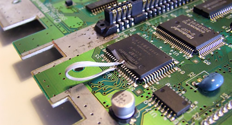
What do you do when you’re working with some vintage ICs and one of the tiny legs pops off? That’s what happened to [Kotomi] when working with an old Super Nintendo. A single lead for the sound chip just snapped off, leaving [Kotomi] one pin short of a working system (the Google Translatrix). This is something that can be fixed, provided you have a steady hand and a rotary tool that’s spinning at thousands of RPM.
Fixing this problem relies on a little bit of knowledge of how integrated circuits are built. There’s a small square of silicon in there, but this tiny die is bonded to a metal leadframe, which looks like the ribcage of a robotic centipede. This leadframe is covered in epoxy, the pins are bent down, and you have an IC. Removing just a tiny bit of epoxy grants access to the leadframe which you can then solder to. Don’t breathe the repair, it’s not pretty, but it does work.
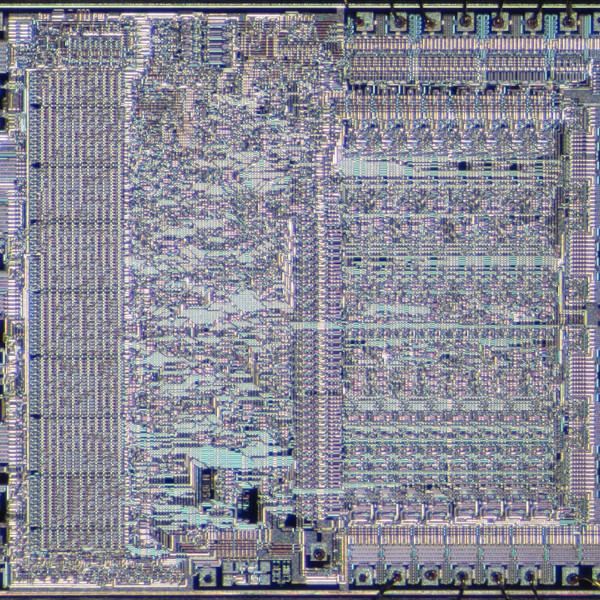
While this technique makes use of a Dremel to break into the chewy nougat center of a vintage chip, and in some ways this could be called decapsulation, it really isn’t. We’ve seen people drop acid to get to the center of a chip and a really hot torch will get to the middle of a ceramic chip, but this technique is just accessing the lead frame of the IC. All ICs have a stamped (or photoetched) metal frame to which the silicone die is bonded. Running a Dremel against some epoxy doesn’t access the silicon, but it does grant access to the signals coming off the chip.


I guess I’m getting old when a surface mount chip like that gets called a “vintage IC”.
You’re not getting old, you’re getting vintage!
Are you old enough to remember when “people drop acid” had an entirely different meaning?
B^)
I’m pretty sure it still does. The question is did Brian mean to reference that? I think so because his phrasing is pretty awkward. Who would word it that way?
Maybe he has been watching “The Men who Stare at Goats”. Perhaps he wants to remote-view a die without ruining the chip?
Good luck Brian. I’m eager to hear about your “progress”. Meanwhile I think I will stick with more conventional methods.
+ a lot.
We had them back in the early 80’s. I know my Tandy 100 has them (6116 RAM chips), I’ve seen them in other devices. A lot of the low volume systems or cheap systems were dip bu the next step up was surface mount. I’m betting they had them in the 70 and I thought I saw some areo-space stuff from the 60’s with surface mount (but not quite high pin count quad pack).
Yep lol..
I’ve done that with dip packages in the past – just grind enough epoxy back to get a solder joint and all is well with the world
“one of the tiny legs pops off”
They have a mind of their own, don’t they.
Sony chip on a Nintendo? Must be a built in feature so that PlayStation rule.
You *are* aware that Sony designed the Super Nintendo’s entire sound subsystem, right?
The SNES sound chips were a first collaboration between Nintendo and Sony. The two went on to begin development of a “SNES-CD” system/add-on. That partenrship fell apart, and Sony decided it would build what would later be the PS1.
https://hackaday.com/2016/07/16/tearing-apart-the-nintendo-playstation/
“All ICs have a stamped (or photoetched) metal frame to which the silicone die is bonded.”
Chip scale packages don’t have leadframe. Though they also have silicon, not silicone die :)
from google translatderp:
“That’s what I want to talk about: fleas made unusable because of a broken flap.”
…nice!
“We’ve seen people drop acid to get to the center of a chip ”
That’s trippy.
Several years ago when the gamecube was all the rage. I had a version of the that has the debuglines cut off the chip which the modchip use. I never had the courage to do this and connect the modchip. Today I would be more confident to do it, but I lack the time and a DVD burner to make use of it.
I courageously (and successfully) performed this on my brand new Wii back when it came out. Had to rebuild 3 legs (out of like 16 per side) off of the optical drive controller chip which was about the size of a nickel. I didn’t know they had done the same thing earlier with the Gamecube.
Cool hack, the only thing I don’t get is why add half a meter of cable to join something 2mm away???
If you don’t, the heat from soldering one end will cause the other end to unsolder!
Not if you are careful, the wires are pretty thin and don’t carry much heat. stuff like this is used all the time in RF prototypes:
https://www.dropbox.com/s/twj0m6la0is0c10/2017-05-27%2022.02.25.jpg?dl=0
Maybe it was what he is confortable working with, but yes, a little piece of tinned wire could be installed instead of that larger wire. But if it works, that is the point.
Also works as an antenna, time delay, or lifting eye.
or, gimmick capacitor (TM)
The trick is to use it to your advantage. Solder the PCB pad first while leaving an inch or so in the opposite end dangling in air. This stub now act as heatsink to the pad when you work on the lead frame side. When you are done, trim it with a knife.
The point is that: the chances that it remains working are highly improved with thinner wires…
And many layers of super-glue. (but mind your eyes when you have to solder it again when covered in super-glue)
Solderwick dismantled is good for this.
Question is when he used such a tool was the proper procedures and safety were implemented?
Bet that didn’t work well afterwards. And damaged to the board and part was unseen to the eye.
And if it did work, it didn’t work for very long.
Can you say ESD Damage?
What is “don’t breathe the repair”? I don’t understand.
Kotomi…? The french one? This guy is a Genius. Just search his console mods on Google…!