The MESM-6 project is focused on bringing the 1960s Soviet BESM-6 computer to the modern age of FPGAs and HDLs. At the moment the team behind this preservation effort consists out of [Evgeniy Khaluev], [Serge Vakulenko] and [Leo Broukhis], who are covering the efforts on the Russian-language project page.
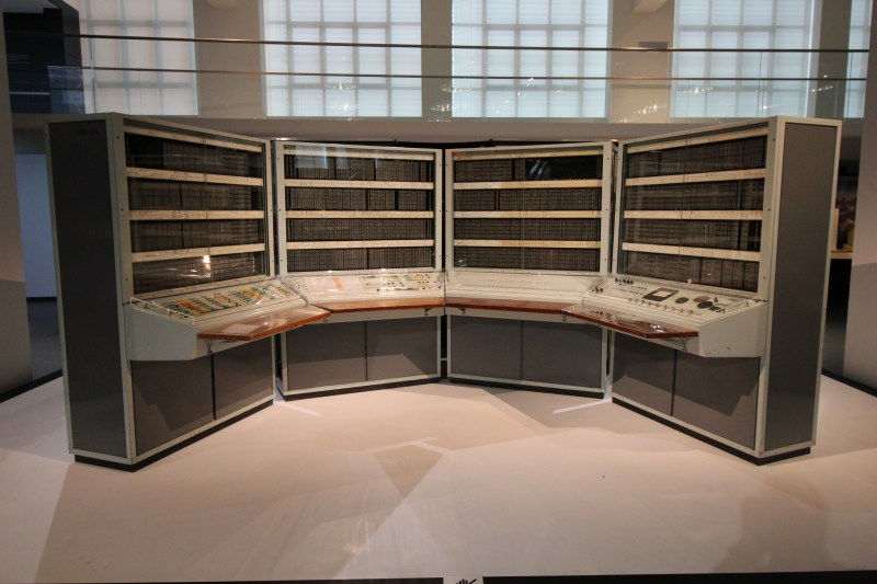
The BESM-6 (in Russian: БЭСМ-6, ‘Bolshaya Elektronno-Schetnaya Mashina’ or ‘large electronic computing machine’) was a highly performing Soviet super computer that was first launched in 1968 and in production for the next 19 years. Its system clock ran at 9 MHz using an astounding number of discrete components, like 60,000 transistors and 170,000 diodes, capable of addressing 192 kB of memory in total. Of the 355 built, a few survive to this day, with one on display at the London Science Museum (pictured above). Many more images and information can be found on its Russian Wikipedia page.
For those not gifted with knowledge of the Russian language, the machine-translated summary reveals that the project goal is to make a softcore in SystemVerilog that is compatible with user mode BESM-6, using the same Pascal compiler as originally used with that system. Further goals include at least 24 kB of data memory, 96 kB of command memory and the addition of modern peripherals such as SPI and I2C.
The system is meant to be integrated with the Arduino IDE, using the Pascal compiler to make it highly accessible to anyone with an interest in programming a system like this. Considering the MIT license for the project, one could conceivably use a bit of Soviet-era computing might in one’s future FPGA efforts.
If after watching the BESM-6 video — included below — you feel inspired to start your own Soviet-computing project, we’d like to wish you luck the Russian way: Ни пуха ни пера!
Прохождение теста БЭСМ-6 (запись от 2008 года). https://t.co/SVF1HEVUoF pic.twitter.com/ZY4cDDmC8T
— x86128 (@x86128) April 18, 2018


I wonder if it would get better performance if the C formation of it because a more cray like shape instead.
That is if its max processing speed is limited by the latency of the connections. Otherwise signal integrity might also benefit and give it a bit more performance.
Though, not having touched or read about one of these before, I have no clue and could only make assumptions.
There are more detailed information about clock signals (in Russian) https://1500py470.livejournal.com/362918.html
Signals are synchronised with analog delay lines. Machine used posedge and negedge logic, almost in ALU.
The 4 panels, left to right, are:
– TLB, write cache and RAM interface;
– CU, data/instruction prefetch, and index registers
– the accumulator and the ALU
– I/O registers and interfaces
Thus there was no need to connect non-adjacent panels, and no advantage from the C configuration. At some installations the panels were arranged in a straight line.
9 MHz is pretty impressive for 1968, assuming that number isn’t from a later generation.
I keep thinking there was something that was supposed to be one of those, or at least reminiscent on “The Americans” show.
This was possible because base machine unit “Блок У” (those with blinking lights) used four different voltage sources to continuously support saturated mode of each bipolar transistor (minimising switch time).
More information (in Russian) https://1500py470.livejournal.com/335675.html
9 MHz was the nominal frequency since the start of production. Originally the 10 MHz frequency was envisioned (some documents mention it), but to work reliably at that frequency, the ambient temperature had to be around 15C/60F, and (anecdotally) that was deemed not acceptable for the sake of operators’ health.
The SIMH project has a software emulator, if you want to play with the architecture and instruction set before the HW is read: https://github.com/simh/simh
Here’s a BESM-6 “Fan” page, mnight be interesting.
http://www.mailcom.com/besm6/
Also main discussion blog (in Russian) of MESM-6 project is https://besm6.dreamwidth.org
Small tests can be run online at http://mailcom.com/besm6/runitnew.cgi
This is amazing!!! Wonder if anyone would ever do the same for ЦВК…