For years I’ve been trying to wrap my mind around how silicon chips actually work. How does a purposefully contaminated shard of glass wield control over electrons? Every once in a while, someone comes up with a learning aid that makes these abstract concepts really easy to understand, and this was the case with one of the booths at Maker Faire Bay Area. In addition to the insight it gave me (and hundreds of Faire-goers), here is an example of the best of what Maker Faire stands for. You’ll find a video of their presentation embedded below, along with closeup images of the props used at the booth.
The Uncovering the Silicon booth had a banner and a tablecloth, but was otherwise so unassuming that many people I spoke with missed it. Windell Oskay, Lenore Edman, Eric Schlepfer, John McMaster, and Ken Shirriff took a 50-year-old logic chip and laid it bare for anyone who cared to stop and ask what was on display. The Fairchild μL914 is a dual NOR gate, and it’s age matters because the silicon is not just simple, it’s enormous by today’s standards making it relatively easy to peer inside with tools available to the individual hacker.
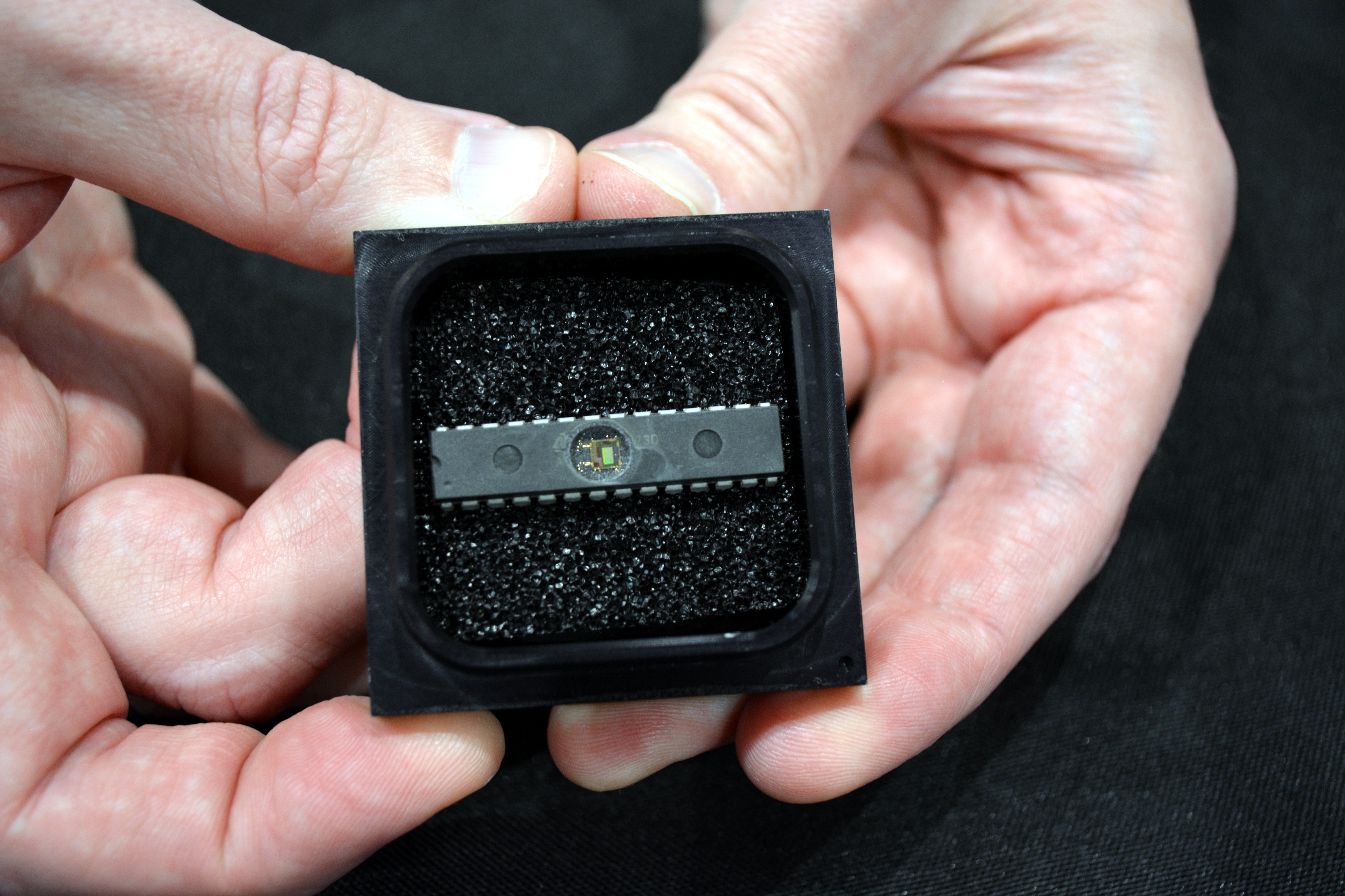
The first challenge is just getting to the die itself. This is John McMaster’s specialty, and you’re likely familiar from his Silicon Pr0n website. He decapped the chip (as well as an ATmega328 which was running the Arduino blink sketch with it’s silicon exposed). Visitors to the booth could look through the microscope and see the circuit for themselves. But looking doesn’t mean understanding, and that’s where this exhibit shines.
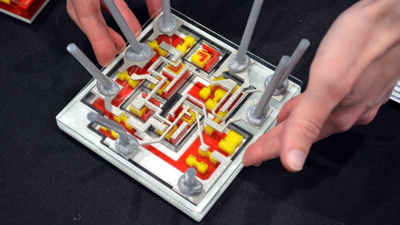
To walk us through how this chip works, a stack-up of laser-cut acrylic demonstrates the base, emitter, and collector of a single transistor. The color coding and shape of this small model makes it easy to pick out the six transistors of the 941 on a full model of the chip. This lets you begin to trace out the function of the circuit.
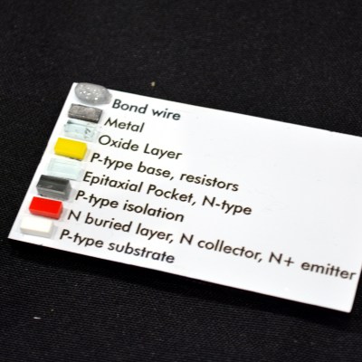
 For me, a real ah-ha moment was the resistors in the design. A resistive layer is produced by doping the semiconductor with impurities, making it conduct more poorly. But how do you zero-in on the desired resistance for each part? It’s not by changing the doping, that remains the same. The trick is to make the resistor itself take up a larger footprint. More physical space for the electrons to travel means a lower resistance, and in the model you can see a nice fat resistor in the lower right. The proof for these models was the final showpiece of the exhibit as the artwork of the silicon die was laid out as a circuit board with discrete transistors used to recreate the functionality of the original chip.
Windell takes us through the booth presentation in the video below. I think you’ll be impressed by the breakdown of these concepts and how well they aid in understanding. This was a brilliant concept for an exhibit; it brought together interdisciplinary experts whom I respect and whose work I follow, and sought to invite everyone to gain a better understanding of the secrets hiding in the chips that underpin this technological age. This is exactly the kind of thing I love to see at a Maker Faire.


This is a great teaching aid. I absolutely love it. Good work to everyone involved, Thank you for the time put in.
Here here!
I can imagine a nice collection of instructions for building a teaching aid out of Legos, or similar block based construction system, for numerous different dies.
Add in a detailed write up of how the circuit works in relation to the model and the topic might be accessible to a wider audience.
Excellent teaching aid. Well done time and effort. Maybe more attractive to add led strip lights to mimic the electron flow when in different states.
There are 6 transistors shown inside the μL914, but only 4 are used in the dual NOR gate, and at least 5 of the 12 resistors are unused. Was that so different metal layers could be used to repurpose the same silicon design for multiple products or was it to add fault tolerance so that if resistors/transistors are faulty a different metal layer could be used to sell the device anyhow or even a bit of both. Like maybe before the metal layer is added, if there was higher demand, a different metal layer could be used and the same underlying silicon sold as three NOT gates, or dual NAND gates, or ….
It was on a standard 8 pin header. There were other devices in the range with different numbers of inputs, and dividers.
I have built several circuits using RTL and they are all horribly unreliable as there is virtually no noise immunity.
Old Intel datebooks explain the manufacturing process quite well, before all enhancements needed to follow Moore’s Law. Those cloud the fundamentals. I’ve always found the really old Fairchild videos some of the best.
https://www.youtube.com/watch?v=RT8XpZVDoAU
But even those already talk about diffusion (or implant nowadays) to dope the crystal, and that’s “just” a refinement in itself (but a very welcome one). The first transistors didn’t have that.
Ok, so, like magic?
side note: Lenore and Windell are the team from Evil Mad Scientist (https://www.evilmadscientist.com/)
It’s more straightforward than that, the transistors are just little flapper valves for the magic smoke.
Silicon is not glass. Silicon dioxide is glass.
A very nice explanation and a well chosen device to start with. Thanks for posting
Brings back memories.
The first IC I ever saw, handled and owned was a uL914 dual two-input NOR gate in an epoxy capped ceramic package about 1964. I took it to school and showed it around telling everyone who would listen that it contained 4 transistors and 6 resistors. They were all terribly unimpressed. It later became a 100 kHz crystal frequency marker using the transistors in a multivibrator from a design in the Technical Topics column of the RSGB Bulletin.
Happy days!
Hope my wife and my friends and family don’t see this. They might ask “is this all you did when you went to work all these years? “. Why would anyone pay you to do this year in and year out, allowing you to play with stuff that’s nothing more than LEGO blocks? And even get paid for it and afford to live in Silicon Valley—on a hill in Cupertino CA where the average home costs $2M??? Makes no sense!
Reminds me of my time in college 5 years ago when my professor thought the best way to teach us how semiconductors was to spend 2 weeks explaining slide rules.
I still to this day don’t completely understand transistors.
In college, I once had the feeling I completely understood transistors. It didn’t last…
The colorscheme reminds me of this :)
http://www.zachtronics.com/kohctpyktop-engineer-of-the-people/
To be fair most chips these days are built with FETs rather that bipolar transistors – FETs are a whole lot easier to explain (and decode) than bipolars
Agreed that classics are sometimes the best material for learning a technology, they usually explain everything thoroughly even if the details are only approximated. Modern works often gloss over important details, only teach outcomes instead of teaching processes that led to exploring those outcomes, or present too many complex equations without relating them to reality or providing useful insight to the numbers. Too much detail at first is overwhelming, newtonian mechanics suits many problems just fine when quantum mechanics isn’t needed.
For that reason, classics such as Schockley’s Electrons and Holes in Semiconductors are irreplaceable, and often divulge insights about the experiments that lead to the formulas and the insights that led to discoveries. Did you know the discovery of the Hall effect led to the intuition that it was possible to create a solid state amplifier using that effect, which eventually led to the invention of the transistor?
I just wouldn’t have called the transparent area between the collector and the base a “gap”, since it is lightly doped but still doped. For the same reason, probably it shouldn’t be transparent in the first place…
Thanks for pointing this out. This cleared the dilemma of how the basics of an IC.
To increase the resistance you can make the trace narrower or longer. Minimum width is determined by the current which needs to flow through it or by process limitations on layer dimensions. R = L / W * {ohms per square determined by the doping level).