Rebuilding The First Digital Personal Computer

When thinking of the first PCs, most of us might imagine something like the Apple I or the TRS-80. But even before that, there were a set of computers that often had no keyboard, or recognizable display beyond a few blinking lights. [Artem Kalinchuk] is attempting to recreate one of these very early digital computers, the Kenbak-1, using as many period-correct parts as possible.

Considered by many to be the world’s first personal computer, the Kenbak-1 was an 8-bit machine with 256 bytes of memory, using TTL integrated circuits for the logic as there was no commercially available microprocessor available at the time it was designed. For [Artem]’s build, most of these parts can still be sourced including the 7400-series chips and carbon resistors although the shift registers were a bit of a challenge to find. A custom PCB was built to replicate the original, and with all the parts in order it’s ready to be assembled and put into a case which was built using the drawings for the original unit.

Although [Artem] plans to build a period-correct linear power supply for this computer, right now he’s using a modern switching power supply for testing. The only other major components that are different are the status lamps, in this case switched to LEDs because he wasn’t able to source incandescent bulbs that drew low enough current, and the switches which he’s replaced with MX-style keys. We’ll stay tuned as he builds and tests this over the course of several videos, but in the meantime if you’re curious how this early computer actually worked we featured an emulator for it a while back.

Continue reading “Rebuilding The First Digital Personal Computer”

Hair Today Gone Tomorrow: Four Men Go To Fix A Wafer Prober

I’ve had a fairly varied early part of my career in the semiconductors business: a series of events caused me to jump disciplines a little bit, and after one such event, I landed in the test engineering department at Philips Semiconductors. I was tasked with a variety of oddball projects, supporting engineering work, fixing broken ATE equipment, and given a absolute ton of training: Good times!  Here’s a story that comes straight off the oddball pile.

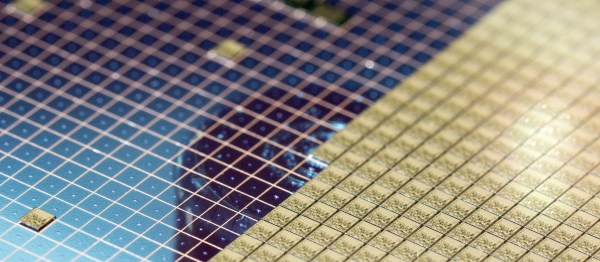
We needed to assemble a crack team of experts and high-tail it to deepest darkest Wales, and sort out an urgent production problem. The brief was that the wafer probe yield was disastrous and the correlation wafer was not giving the correct results. Getting to the punch line is going to require some IC fabrication background, but if you like stories about silicon, or red-bearded test engineers, it’s worth it. Continue reading “Hair Today Gone Tomorrow: Four Men Go To Fix A Wafer Prober”

Developing The First ICs In Orbit

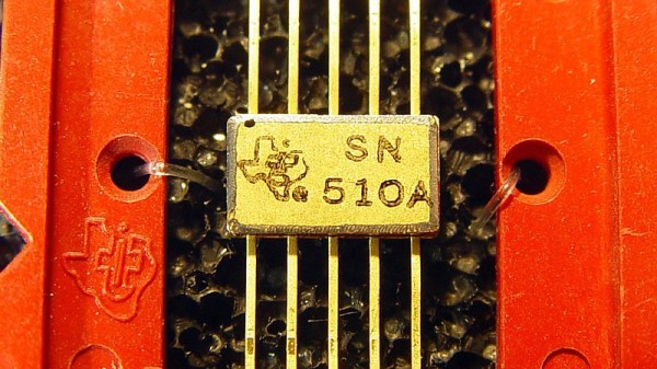
Over six decades of integrated circuit production we’ve become used to their extreme reliability and performance for a very reasonable price. But what about those first integrated circuits from the early 1960s? Commercial integrated circuits appeared in 1961, and recently Texas Instruments published a fascinating retrospective on the development of their first few digital ICs.

TI’s original IC product on the market was the SN502, a transistor flip-flop that debuted at $450 (about $4100 today), which caught the interest of NASA engineers who asked for logic functions with a higher performance level. The response was the development of the 51 series of logic chips, whose innovation included on-chip interconnects replacing the hand interconnects of the SN502. Their RCTL logic gave enough performance and reliability for NASA to use, and in late 1963 the Explorer 18 craft carried a telemetry system using the SN510 and SN514 chips into orbit. 52 and 53 series chips quickly followed, then in 1964 the 54 series TTL chips which along with their plastic-encapsulated 74 series equivalents are still available today.

Considering that in 1961 the bleeding edge of integrated circuit logic technology was a two-transistor chip with hand interconnects, it seems scarcely conceivable that by ten years later in 1971 the art had advanced to the point at which the first commercially available microprocessors would be produced. It’s unlikely that many of us will stumble upon any of the three-figure SN1-series logic chips, but to read about them is a fascinating reminder of this pivotal moment in the history of electronics.

Header: Mister rf, CC BY-SA 4.0.

What To Know When Buying Chips That Haven’t Been Made For Three Decades

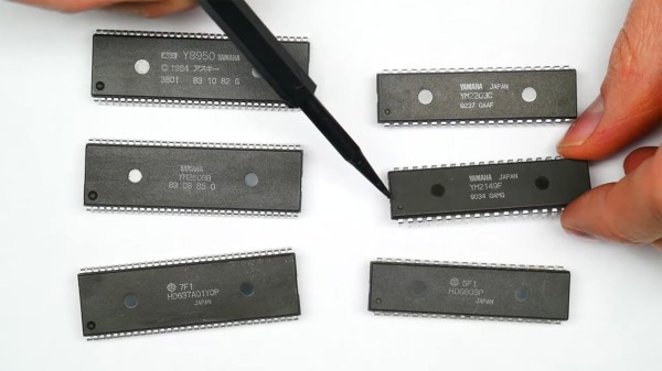
Those of us who have worked with vintage sound generator chips such as the Yamaha FM synthesizers in recent years have likely run into our own fair share of “fake” or “remarked” chips, sometimes relabeled to appear as a chip different than the die inside the packaging entirely. [David Viens] from Plogue has finally released his findings on the matter after 3 years of research. (Video, embedded below.)

The first thing to determine is in what way are these chips “fake”? Clearly no new YM2612’s were manufactured by Yamaha in 2015, but that doesn’t mean that these are simply unlicensed clones put out by another die factory. [David] explains how these chips are often original specimens sourced from recycled electronic waste from mostly environmentally unsafe operations in China, which are then reconditioned and remarked to be passed as “new” by resellers. Thankfully, as of 2017, he explains that most of these operations are now being shut down and moved into an industrial park where the work can be done in a less polluting manner.

The next thing that [David] dives into is how these remarked chips can be spotted. He explains how to use telltale signs in the IC packaging to identify which chip plant produced them, and visible indications of a chip that has been de-soldered from a board and reconditioned. There are different ways in which the remarking can be done, and sometimes it’s possible to undo the black-top, as it’s called, and reveal the original markings underneath with the simple application of acetone with a cotton swab.

We’ve talked about fake chips and how they can lead to hardware failure here before, but in the case of chips like these which aren’t manufactured anymore, we’re not left with much choice other than FPGA or software reimplementations. Check out [David]’s 40-minute look into these chips after the break.

Continue reading “What To Know When Buying Chips That Haven’t Been Made For Three Decades”

The Golden Age Of Ever-Changing Computer Architecture

Given the accuracy of Moore’s Law to the development of integrated circuits over the years, one would think that our present day period is no different from the past decades in terms of computer architecture design. However, during the 2017 ACM Turing Award acceptance speech, John L. Hennessy and David A. Patterson described the present as the “golden age of computer architecture”.

Compared to the early days of MS-DOS, when designing user- and kernel-space interactions was still an experiment in the works, it certainly feels like we’re no longer in the infancy of the field. Yet, as the pressure mounts for companies to acquire more computational resources for running expensive machine learning algorithms on massive swaths of data, smart computer architecture design may be just what the industry needs.

Moore’s law predicts the doubling of transistors in an IC, it doesn’t predict the path that IC design will take. When that observation was made in 1965 it was difficult or even impossible to envision where we are today, with tools and processes so closely linked and widely available that the way we conceive processor design is itself multiplying.

Continue reading “The Golden Age Of Ever-Changing Computer Architecture”

Integrated Circuits Can Be Easy To Understand With The Right Teachers

For years I’ve been trying to wrap my mind around how silicon chips actually work. How does a purposefully contaminated shard of glass wield control over electrons? Every once in a while, someone comes up with a learning aid that makes these abstract concepts really easy to understand, and this was the case with one of the booths at Maker Faire Bay Area. In addition to the insight it gave me (and hundreds of Faire-goers), here is an example of the best of what Maker Faire stands for. You’ll find a video of their presentation embedded below, along with closeup images of the props used at the booth.

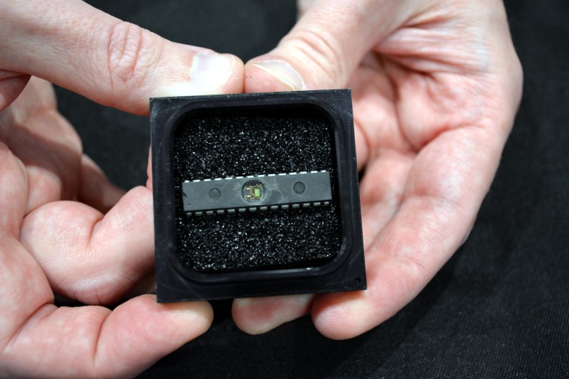
The Uncovering the Silicon booth had a banner and a tablecloth, but was otherwise so unassuming that many people I spoke with missed it. Windell Oskay, Lenore Edman, Eric Schlepfer, John McMaster, and Ken Shirriff took a 50-year-old logic chip and laid it bare for anyone who cared to stop and ask what was on display. The Fairchild μL914 is a dual NOR gate, and it’s age matters because the silicon is not just simple, it’s enormous by today’s standards making it relatively easy to peer inside with tools available to the individual hacker.

ATmega328 decapped by John McMaster was also on display at this booth

The first challenge is just getting to the die itself. This is John McMaster’s specialty, and you’re likely familiar from his Silicon Pr0n website. He decapped the chip (as well as an ATmega328 which was running the Arduino blink sketch with it’s silicon exposed). Visitors to the booth could look through the microscope and see the circuit for themselves. But looking doesn’t mean understanding, and that’s where this exhibit shines.

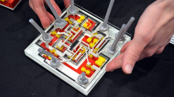
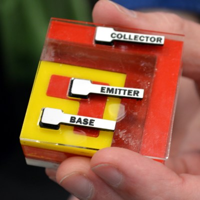
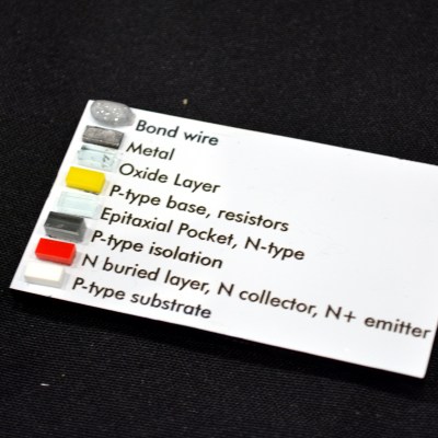
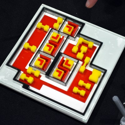
To walk us through how this chip works, a stack-up of laser-cut acrylic demonstrates the base, emitter, and collector of a single transistor. The color coding and shape of this small model makes it easy to pick out the six transistors of the 941 on a full model of the chip. This lets you begin to trace out the function of the circuit.

For me, a real ah-ha moment was the resistors in the design. A resistive layer is produced by doping the semiconductor with impurities, making it conduct more poorly. But how do you zero-in on the desired resistance for each part? It’s not by changing the doping, that remains the same. The trick is to make the resistor itself take up a larger footprint. More physical space for the electrons to travel means a lower resistance, and in the model you can see a nice fat resistor in the lower right. The proof for these models was the final showpiece of the exhibit as the artwork of the silicon die was laid out as a circuit board with discrete transistors used to recreate the functionality of the original chip.

Windell takes us through the booth presentation in the video below. I think you’ll be impressed by the breakdown of these concepts and how well they aid in understanding. This was a brilliant concept for an exhibit; it brought together interdisciplinary experts whom I respect and whose work I follow, and sought to invite everyone to gain a better understanding of the secrets hiding in the chips that underpin this technological age. This is exactly the kind of thing I love to see at a Maker Faire.

Continue reading “Integrated Circuits Can Be Easy To Understand With The Right Teachers”

Ken Shirriff Chats About A Whole World Of Chip Decapping

Reverse engineering silicon is a dark art, and when you’re just starting off it’s best to stick to the lesser incantations, curses, and hexes. Hackaday caught up with Ken Shirriff at last year’s Supercon for a chat about the chip decapping and reverse engineering scene. His suggestion is to start with an old friend: the 555 timer.

Ken is well-known for his work photographing the silicon die at the heart of an Integrated Circuit (IC) and mapping out the structures to create a schematic of the circuit. We’re looking forward to Ken’s talk in just a few weeks at the Hackaday Superconference. Get a taste of it in the interview video below.

Continue reading “Ken Shirriff Chats About A Whole World Of Chip Decapping”