It’s tough to find a project these days that doesn’t use an analog-to-digital converter (ADC) or digital-to-analog converter (DAC) for something. Whether these converters come as built-in peripherals on a microcontroller, or as separate devices connected over SPI, I2C, or parallel buses, all these converters share some common attributes, and knowing how to read the specs on them can save you a lot of headaches when it comes to getting things working properly.
There are some key things to know about these devices, and the first time you try to navigate a datasheet on one, you may find yourself a bit confused. Let’s take a deep dive into the static (DC) properties of these converters — the AC performance is complex enough to warrant its own follow-up article.
The Two Domains
Think of digital pins on a microcontroller. The value of the pin can be a 1 or a 0 and it’s easy to understand that the voltage for those values will be zero volts or five volts (assuming our microcontroller is powered by a five volt source). What about all those voltages in between? If we need to measure or generate a signal anywhere in between the zero and five volt levels we’re going to need an ADC or DAC. But there are myriad different uses for the two.
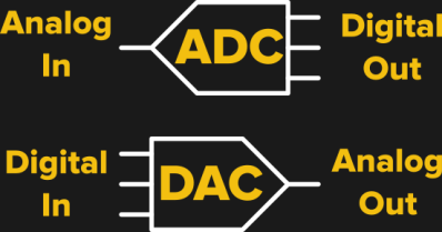
 The obvious purpose of these converters is to translate a quantity between analog and digital domains. Shown in the figure are two hypothetical 3-bit converters, one of each type. For simplicity, we’ll assume a straight binary encoding on the digital side, with ‘000’ corresponding to the smallest output and ‘111’ the largest. Other converters may use a signed or offset binary representation, or other more complex codes (PDF). Either way, the digital side, be it input or output, is pretty straightforward. In the case of an N-bit straight binary converter, the digital side consists of 2N values, from 0 to 2N-1. Note that 2N itself is not in the set; our 3-bit converter stops at 7.
The analog side, on the other hand, can be more complex. For starters, the analog quantity can be a voltage, a current, or in the case of digital potentiometers, a resistance. In the case of voltage or current converters, the output may be single ended — that is, carried on a single wire — or differential, with the analog quantity being the difference between two inputs or outputs. But, underlying this diversity is a common set of properties — and specifications — that’s important for understanding and applying these converters.
Digital To Analog
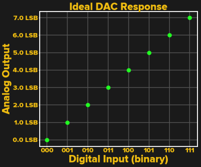
 For the simple 3-bit DAC described above, we can create an idealized plot of the transfer function — this is simply the relationship of input (a digital value) to output (an analog value). The digital value, on the x-axis, obviously takes on only certain values, indicated in binary on the plot. The y-axis is a little more confusing. It’s common in specifications to describe the analog side in units of LSB, corresponding to the smallest step of the converter — in other words, units of the analog value of the least significant bit. This at first seems like an odd way to describe an analog quantity, but there’s a good reason for it.
Almost all converters allow the designer to specify a reference value for the full-scale output. For instance, we might choose the full-scale output of a DAC to be 7 V in one circuit. In that case, the LSB would be 1 V. Also note that to get a 7 V full-scale output, we must use an 8 V reference voltage for the DAC: the maximum output is Vref * x / 2N, where x is the binary input code. Note that your converter may vary: always read the datasheet to be sure.
In another circuit using this example DAC, we might choose a full-scale value of 3.5 V, so the LSB would be 0.5 V. So, the real-world resolution of the converter depends on the reference voltage. As it turns out, a number of other important parameters — especially errors — also depend on the reference, so listing them in LSB units in the datasheet allows an easy comparison and conversion to real-world units: a simple multiply does it.
Errors
One of the places you’ll see LSB units turning up is in non-linearity error specifications. Shown below is an excerpt from the datasheet for my go-to DAC for low-frequency use, the 12-bit voltage-output MCP4821 (PDF) from Microchip (they use LSb with a lower-case “b”, but I won’t hold it against them). Two other new terms also show up here — INL, or integral non-linearity, and DNL, or differential non-linearity. Even though they sound like you’ll have to dust off your old calculus textbook, don’t worry, these are both simple concepts.
DNL is simply the difference between an ideal LSB valued step size and what you’ll actually see from the device. In the case of the MCP4821, the ±0.25 LSB specification says that the actual step sizes will all be between 0.75 LSB and 1.25 LSB. In our 3-bit/7 V converter example, we can expect each step to be between 0.75 V and 1.25 V. (Footnote to the pedantic: the DNL specification is in the “typical” column of the datasheet, so you may actually see better or worse values). For large values of DNL, exceeding 1 LSB, the DAC can become non-monotonic, meaning that the output may decrease as the input increases in some interval; this is definitely something you need to be aware of.
INL, on the other hand, measures the maximum difference between an ideal straight-line transfer function and the actual one. For example, if the actual points lie along a curved or irregular path, the INL tells you how far off from the ideal value you can be at any point. For example, the ±4 LSB INL spec above would be terrible for our toy 3-bit / 7V converter, implying the output could be off by up to 4 V. For a 12-bit DAC, however, this is a much more respectable spec, implying less than 0.1% error (4 / 4095). Don’t make the mistake of taking ±4 LSB and interpreting this as four bits, or 24 = 16 steps.
Analog to Digital
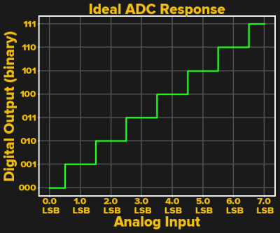
 In the case of ADCs, the inputs and outputs take on reversed roles as shown in the plot of the transfer function for our toy 3-bit ADC. Now, the inputs are described in units of LSB, which may be voltage or current, and the output is a digital value, in this case a straight binary representation. As one would expect, the output code changes in jumps as the input value crosses successive thresholds. What may not be obvious at first is that the ideal thresholds are at half-steps, and the input range corresponding to the smallest and largest digital outputs are half the size of the others. The threshold between ‘000’ and ‘001’, for instance is set at 1/2 LSB. This minimizes the error in the conversion; you can think of this as “rounding” to the nearest output value.
Note that if we want our LSB value to be 1 V for this example ADC, we use an 8 V reference voltage. This sets the lowest threshold at 0.5 V, and the largest threshold at 6.5 V. This is a typical arrangement for ADCs, but this is not always the case; some converters have their thresholds at integer multiples of LSB. Always read the datasheet for your part to see exactly how it works.
DNL and INL errors are also specified for ADCs. In this case, the DNL error value specifies the maximum distance between thresholds for successive output values — in other words, the width of the steps in the graph. Again, values of DNL greater than 1 LSB can be problematic in ADCs, causing a symptom known as missing codes: the output may skip certain digital values entirely. As with DACs, in ADCs, INL error tells you the maximum distance of any threshold to the ideal straight line conversion, in other words, how far away from the expected value you can be.
There’s another “error” associated with ADCs: quantization error. I’ve thrown quotes around the word here because quantization error isn’t a deviation from the ideal ADC model. Instead, it’s simply a result of the discrete digital steps of the output. Since the input can have any analog value, there can be up to 1/2 LSB of error when this is converted to a digital value in discrete steps. For instance, an analog input value of 1/2 LSB plus an arbitrarily tiny amount will be converted as digital ‘001’, while an input of 1/2 LSB minus an arbitrarily tiny amount will be converted as ‘000’. Either one differs from the original input value by around 1/2 LSB.
Gain and Offset Error
The final two errors you’re likely to see mentioned are gain and offset. Offset error is easy to visualize: the zero point on either transfer function may not correspond to zero in the analog world; a voltage DAC with a digital input of zero may output a non-zero voltage. Gain errors, on the other hand, represent the difference from an ideal transfer slope of 1. For instance, if a voltage-output DAC has an integrated buffer amplifier, the amplifier may not have a gain of exactly 1; in this case, the buffer will cause the output to be high or low, depending on the actual amplifier gain. This is also where errors in a reference voltage show up.
The good thing about gain and offset errors is that they can be easily “calibrated out.” With two measurements of the system, you can determine the actual gain and offset values, and use these values to correct the errors in software. In fact, these are typically the only two errors that you’ll commonly see corrected; for the others, you’ll typically choose a better converter if you need it. TI has a nice video explaining how to do this calibration.
The Bottom Line
So, that’s a quick run-through of the DC (direct current) part of ADC and DAC specifications: the take away should be that you can understand the error in an ADC or DAC by examining the gain, offset, and INL specifications. Hopefully, this gives you enough as a starting point for digging in when you need to. If you want to delve into the details, there are a number of good references published by semiconductor manufacturers. TI’s Understanding Data Converters (PDF) is a great start; Microchip also has a good explanation on their site.


“RTFM” needs to come back into common use. very handy abbreviation.
I use it at work all the time. It seems to be a lost art to read the manual to figure something out for ones self. I could just tell them how to do it but then I have a bunch of robots that are useless when things don’t go exactly as they should; whereas if I show them how to find the information they are better equipped to handle the normality of integration/production, where nothing goes exactly as it should.
The best class I had in the Navy was how to properly read technical manuals.
Also sorry to say the grammar Nazi’s. Numbers always made more sense to me than the intricacies of commas, semicolons, etc..
Binary range is 0 to (2^n)-1, your superscript reads 0 to 2^(n-1)
Thanks! Fixed.
It would be even better if actual manuals came back into common use so that we really could RTFM. Sadly a hastily thrown together barely literate glob of text on a web page and a victims self help forum is considered a suitable substitute for reference documentation, even for some quite expensive CAD software…
I have worked in factories where brand new, megabuck, machinery came with no operation manual, maintenance manual or even a basic description of its normal operation. It shows up in boxes and you put it together like an Interocitor, match the parts to the pictures and hope that it works.
LSB = Least Significant Byte
LSb = Least Significant bit
good thing you don’t speak french…
That’s funny, drhatch. Joe Pesci funny.
LSB is commonly used to mean Least Significant Bit in ADC and DAC specifications.