If you were asked to imagine a particle accelerator, you would probably picture a high-energy electron beam contained within a kilometers-long facility, manned by hundreds of engineers and researchers. You probably wouldn’t think of a chip smaller than a fingernail, yet that’s exactly what the SLAC National Accelerator Laboratory’s Accelerator on a Chip International Program (ACHIP) has accomplished.
The Stanford University team developed a device that uses lasers to accelerate electrons along etched channels on a silicon chip. The idea for a miniature accelerator has existed since the laser’s invention in 1960, but the requirement for a device to generate electrons made the early proof-of-concepts difficult to manufacture in bulk.
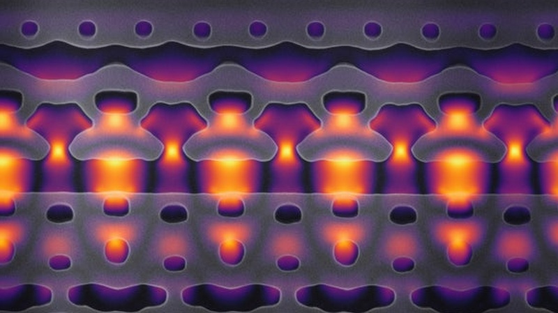
The electromagnetic waves produced by lasers have much shorter wavelengths than the microwaves used in full-scale accelerators, allowing them to accelerate electrons in a far more confined space – channels can be shrunk to three one-thousandths of a millimeter wide. In order to couple the lasers and electrons properly, the light waves must push the particles in the correct direction with as much energy as possible. This also requires the device to generate electrons and transmit them via the proper channel. With an accelerator engraved in silicon, multiple components can fit on the same chip.
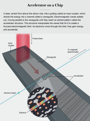
Within the latest prototype, a laser hits a grating from above the chip, directing the energy into a waveguide. The electromagnetic waves radiate out, moving with the waveguide until they reach an etched pattern that creates a focused electromagnetic field. As electrons move through the field, they accelerate and gain energy.
The results showed that the prototype could boost the electrons by 915 electron volts, equivalent to the electrons gaining 30 million electron volts over a meter. While the change is not on the scale of SLAC, it does scale up more easily since researchers can fit multiple accelerating paths onto future designs without the bulk of a full-scale accelerator. The chip exists as a single stage of the accelerator, allowing more researchers to conduct experiments without the need to reserve space in expensive full-scale particle accelerators.


So now, do they get “bunching” of the electrons within the accelerator also?
Based on my very limited understanding of the technology and the basic concept in the video, I would think there would be “bunching”.
At its core, it’s much like the microwave system and still has high and low nodes…but at a higher frequency. So probably smaller “bunches” at a higher frequency.
Yes, unfortunately the optical accelerators need MUCH smaller, tighter bunches than microwave accelerators work with (and produce much smaller, tighter bunches as well!). So they’ve tried using SLAC as a source (early papers), and building smaller sources to do more frequent testing without a full mile of beam forming and a power bill the size of Texas.
See https://achip.stanford.edu/publications for some of the published efforts, and the article above for details of current experimental setups.
Thanks for post, been looking into these issues for about 10 years, few anomalies pop up now and then, many unresolved…
Now combine above with an electrically modulated neutron flux source (neutristor) easily scalable, you might well have a home nuclear source of sorts. If in an electrochemical cell (cold fusion paradigm) and appropriate metallurg/topology for best QM fit you might just get close enough to produce useful energy overall:-
[Link to YouTube video on neutristor disabled two previous attempts to post, so] here is a related web page:-
https://newatlas.com/sandia-neutristor-neutron-generator-chip/23856/
I wanted to get a neutristor so I could make a nuclear furnace, but I couldn’t find a source for concentrated thorium.
http://ecoralph.blogspot.com/2013/06/nuclear-furnace-for-home-heating.html
Coleman white gas lamp mantles but it will take more than a few of them.
You need some luck, as Thorium is more and more phased out due to radiation scare
I live in Western Australia, we have all sorts of mineral sands not just on the coast but inland as well. North of Perth which is our capital there are many white sand beaches. On closer inspection there are a few tiny black particles which I understand is thorium oxide or silicate or some other mix. It might well be easy to separate with the right mix of field strength and frequency from the underlying sand base…
https://link.springer.com/article/10.1007/s12274-013-0379-6
I think there might be a limit on how much separation or rather amount of refined thorium in one mass but, we have heaps of it. I understand it’s also fairly common in India too.
Ocean, lake and river sands I’ve played with, have black particles… which usually come out with a magnet because they’re iron.
>If you were asked to imagine a particle accelerator, you would probably picture a high-energy electron beam contained within a kilometers-long facility, manned by hundreds of engineers and researchers.
I would imagine a CRT.
Yeah… when I think of particle accelerators I think of accelerators that accelerate particles.
And now more countries can afford an accelerator. The democratizing of particle physics.
Yes! And hopefully for enthusiasts, too!
Where can I buy an ACHIP?
Don’t think any are for sale yet (and the laser is still a bit pricey), but check the publications at https://achip.stanford.edu/publications
If a country can’t afford a regular accelerator it can’t afford this thing either. Also, what to use 1 keV for? Pretty useless apart from demo.
PEW PEW PEW
First thing I thought was “with a metal target, it’s a miniature, low voltage x-ray source!”
Using a similar (but not identical – it gets complicated) structure after the accelerator as an undulator, and you have a free electron laser driven by an IR laser, that can produce pulses of hard coherent X-rays at a very high rate.
Or, use a curved magnetic field driven by the same IR laser to bend the beam and you can get synchrotron radiation (ALS on a desktop – and dial a wavelength).
And there’s a good chance that all of that can be built on a single piece of silicon in the near future.
Make for a great part of a lab on a chip.
NACH (Nuke on A CHip)
natch!
B^)
AliExpress version with Bluetooth also integrated in 3… 2…
There is a word for a one-thousandth of a millimeter, Sharon. :)
Yes,
milli-millimeter!
B^)
10 kilo-Angstroms.
So… (seriously)
Might we be seeing ACHIP proton accelerators in the near future?
If we do, would they make a new kind of ion thruster? I wonder what the efficiency would be?
Probably lower efficiency than just using the momentum of the laser beam. Yeah, I already went down that road, and the numbers weren’t great.
But, the ACHIP designs can accelerate protons and ions in a different configuration.