NASA says that Electronic Alchemy’s eForge 3D printer is another space program spinoff. The printer looks a lot like a conventional 3D printer but unlike its mundane cousin it can print sensors, lights, and other electronic components. It does that by using one of six or eight different materials.
Six of the eight spools each have some sort of electronic property. According to the company they have conductive filament, resistive filament, insulating filament, capacitive filament, and both N- and P-type semiconductors.
This strikes us a bit odd though, since we wouldn’t normally think of a filament as having capacitance alone. Perhaps it has a high dielectric constant that becomes the sandwich filling between conductive parts. The same goes for semiconductors, we’d expect an amorphous solar cell might be printable, but we’d expect active devices to usually require a crystalline structure.
According to the NASA post, they have or will have filaments that light up, magnetic materials, and piezoelectric substances. It all sounds great and the videos look interesting, but we will be very intrigued to see how it plays out in practice.
If you think you want one, be prepared. The price looks as though it will start around $10,000 so this won’t be an item in every garage. The filaments are 4mm which is disappointing since they could really be a game-changer if they work as advertised. Even if you had to swap filaments a few times for each layer, if the materials would work in an ordinary printer, there would be a much larger market. We assume the substrate material to be just ordinary PLA or some other thermoplastic. We’d love to see this married with a real PCB mill.


Solid proof that resistance isn’t futile?
Resistance is ductile.
Hey look… we’re not just going to live on the moon and mars… we’ll have the most invasive nuisance remote sensing with remote transmission ever! Totally awesome! What?
Actually, the eight extruders and different filaments seems impressive. Makes me think if they can get really accurate with much smaller size extrusions quantitatively valid with maybe some performance enhancement methods… printing microwave guides or optical like electronics components can be do able. Seems will need more like a ink jet or laser method or other method though maybe layering ink like with different polymers.
There is no specific info on their website about electrical and mechanical properties of 3D printed materials. Actually, they haven’t shown measurements or anything scientific for their work.
it sounds like an investment scam.
All semiconductor devices manufactured today use complicated wafer chemistry wizardry that just does not have an analogue in the kind of manufacturing that FDM 3D printers do, and even the more primitive types of transistor that might, *might* be made with FDM using exotic materials just would not provide the size, speed or power capability of modern transistors.
Even simple components like resistors and capacitors rely on a complex understanding of materials science for precise control of properties like conductivity and relative permittivity.
I could imagine that you might be able to have a “3D printer” that “prints” complex electronic circuits, but somewhere inside of it would be a pick-and-place machine that just puts regular SMD components in there, and even then SMD processes require precision control of dimensions and coordinates that might not like the softness of freshly lain filament.
Yeah FDM doesn’t directly parallel the optics lab setup for even normal sized homebrew transistors.. But that doesn’t mean larger scale and lower performance FDM printed ones won’t have many many uses. I am however doubtful that this will work for much beyond integrating input sensing into prototype builds. If you want a trace or two running on the plastic case components now its a many step awkward process. Just print it integral could be a game changer.
Also have to ask just how recyclable these filaments are, composite materials generally suck for recycling. Though if these are all PLA based that isn’t the end of the world on the hydrocarbon front the additives to get the electronic effects are probably rare, mildly toxic or something else to worry about.
What I’d really like to see is how they explain how they control the schottky barriers where they connect conductive filament to semiconductor filament.
So I found the NASA research proposal:
https://sbir.nasa.gov/SBIR/abstracts/16/sttr/phase2/STTR-16-2-T12.04-9850.html
This isn’t very helpful either; the full description of the plastic is “Several methodologies were explored: (a) direct laser melting of nanopowders onto the surface, (b) an ink-based approach using nanopowder mixtures with fast UV curable epoxy, (c) nanopowder/ABS material mixtures in an acetone solution, and (d) filaments created from a nanopowder and a thermoplastic adhesive”.
On the website blog, they describe a capacitive pressure sensor (https://www.electronicalchemy.com/2019/08/pressure-sensor-test-print/) made as a resistive-capacitive-resistive material stack. This seems to confirm the “capacitive” material is used as a dielectric, and, assuming a dielectric constant of ~4 (a bit better than ABS), using ~20x20mm by 1mm dielectric dimensions, their given time constant of ~4us, and an effective resistor size of ~2x4mm by 10mm, the “resistive” material is ~1e4ohm-cm. Proto-pasta sells 30-100ohm-cm conductive filament (https://www.proto-pasta.com/products/conductive-pla), which implies neither of these eForge materials are improvements on what’s already commercially available (though semiconducting thermoplastic would be quite a trick, if it exists).
If you have to go with a DIY etch method, than printing on inkjet glossy-photo-paper with a laser printer in dark-mode for direct transfer is fairly reliable. I was able to 0.5 mm pitch large QFN packages to wotk rather well.
These days the process is far easier with inexpensive PCB makers like Oshpark, jlpcb, and pcbway.
Dry film is also an option, but YMMV depending on your transparency quality.
—
Does anyone know if the eForge print head retracts the unused nozzles?
We tried a similar side-by-side kit a few years back, and found the cross-contamination from over extrusions made it almost unusable for multi-material printing.
This is the dawning of the diamond age.
Naw, we are still in the sensationalist age for a while
Hot damn! Soon we’ll be able to print our own millimeter-scale transistors!
More like centimeter scale with filament that fat, unless it’s a misprint for 0.4mm.
Filament size != extruded size. My og makerbot cupcake takes 3mm filament but prints at 0.4 mm
Even when you can print finer features than the filament, you would want them to be larger to make up for the poor electrical properties. There are filler/binder material in the filament thus making them inferior to the real thing.
Please check a little bit what you publish.
It’s obvious it’s just another KickStarter scam.
P and N plastics are a joke that makes no sense to anyone who knows a little bit about the basics of electronics.
Here’s an interesting reddit thread on the subject:
https://www.reddit.com/r/shittykickstarters/comments/dte07n/eforge_3d_printer_capable_of_printing/
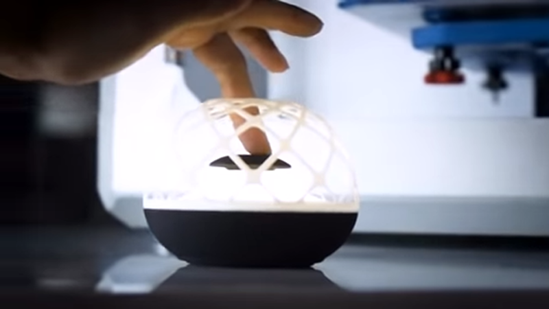
The video makes us believe in a printed lamp that lights up as soon as it comes out of the printer.
In the end they even dare to show a drone !!!
Smells like Kickstarter
what they don’t tell you, is that each of those filaments, costs more than gold, and you’ll screw up half the time because their printer/filament profile isn’t very good, and that setting up zero datum for 8 movable nozzles is much harder than for just one.
ie: i’ll believe it when I see it actually work well.
This looks big for prototyping electronics. I hope it can live up to the hype
…it won’t. and even if it does, see the above comment about cost.