When the Game Boy Advance came on the scene in 2001, it was a pretty big deal. The 32-bit handheld represented the single biggest upgrade the iconic Game Boy line had ever received, not only in terms of raw processing power, but overall design. It would set the state-of-the-art in portable gaming for years, and Nintendo was eager to get developers on board.
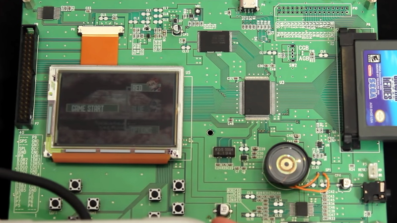
Which could explain why the official GBA development kit, recently shown off by [Hard4Games], looks like something that was built in a hackerspace. It’s pretty common for console development systems to look more like boxy 1990s computers than the sleek injection molded units that eventually take up residence under your television, but they don’t often come in the form of a bare PCB. It seems that Nintendo was in such a rush to get an early version of their latest handheld’s guts out to developers that they couldn’t even take the time to get a sheet metal case stamped out for it.
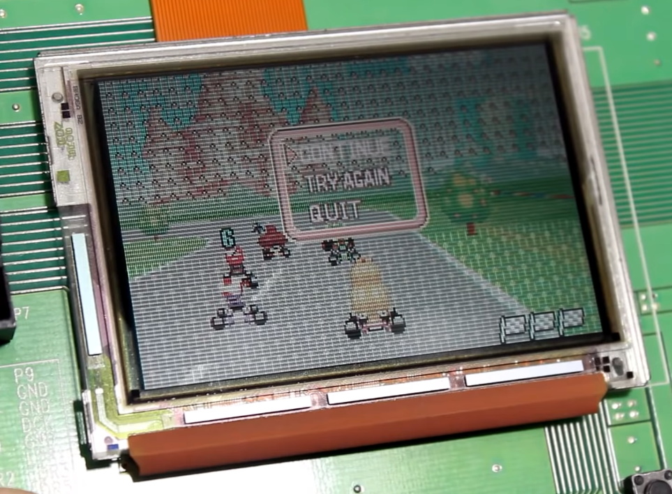
All of the principle parts of the final GBA are here, and as demonstrated in the video after the break, the board even plays commercially released games. Though [Hard4Games] did find that some titles from the later part of the handheld’s life had unusual graphical glitches; hinting that there are likely some low-level differences that don’t manifest themselves unless the developer was really digging deep to squeeze out all the performance they could.
The board also lacks support for Game Boy and Game Boy Color games, though this is not wholly surprising. When an older game was inserted into a GBA, the cartridge would physically depress a switch that enabled a special 8080-based coprocessor that existed solely for backwards compatibility. Adding that hardware to a development board would have made it more expensive and added no practical benefit. That said, [Hard4Games] does point out that there appears to be a unpopulated area of the board where the backwards compatibility switch could have been mounted.
Hackers have always been enamored with the Game Boy, so it’s fitting to see that the official development kit for the final entry into that storied line of handhelds looked a lot like something they could build themselves. If anyone feels inclined to build their own “deconstructed” GBA in this style, you know where to find us.
[Thanks to NeoTechni for the tip.]


Just to get out in front of the potential mud-slinging regarding the “special 8080-based coprocessor” statement from the article: No, it’s not particularly special, and no, it’s not exactly 8080-based. But it’s also not exactly a Z80, either. It’s the Sharp LR35902, which straddles the line and forms a sort of middle ground between the 8080 and the Z80.
It has additional instructions that are found in the Z80, but it lacks some of the more extended ones, and similarly it lacks the swappable set of shadow registers that characterizes the Z80.
“Special” in this context just means it’s an additional part for this specific feature, and isn’t used in normal operation.
I don’t understand the need to specifically define the processor as “8080 plus” or “z80 minus” or “actually it’s not an 8080 or a z80 guys!”. It’s related to both, and whatever description helps you to understand how it works is perfectly fine.
It was an informative reply even if it had a pedantic trigger.
Yep, I remember that dev board from ’99. It’s not as fragile as the video suggests.
It’s an EVT board; the entire point is to get all the functionality present and make it as easy to debug as possible, breaking out all the important signals and using bigger traces and larger pitch parts that are simpler to work with.
By it’s nature it’s going to be less fragile than a DVT or PVT board that has to cram everything together into the final form factor and needs the final case to fully protect everything.
I challenge someone to speedrun a game of their choosing using the on-board buttons.
Challenge accepted!
Send me the board with a Mario Kart cartridge.
B^)
> looks like something that was built in a hackerspace.
If only your average hackspace boards are like these. There are no adruinos type of stacked shields or 9V batteries either. There are no silly through hole only parts, melted/oversized/baldy stripped wires, bad soldering and uncleaned resins.
The boards are professionally layout and assembled on a production line. The only thing they haven’t done is to cram the boards.
Sounds like you’re comparing a novice only working at home with an experienced hacker with the good tooling of a large hackerspace. There’s nothing wrong with being a novice, no one has ever jumped from nothing to years of experience without the years of experience.
None of that is really a huge deal unless you’re trying to sell them to people. There are some potential advantages to through hole parts, especially for prototypes and in development stuff.
Also it takes time to develop good soldering skills and not everyone has the ideal set of tools.