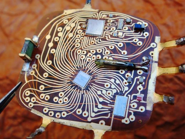
There has been an argument raging for years over whether you should design circuit boards with 45-degree corners or 90-degree corners. Why make them with corners at all? This breathtaking circuit board art is from a digital watch circa 1975.
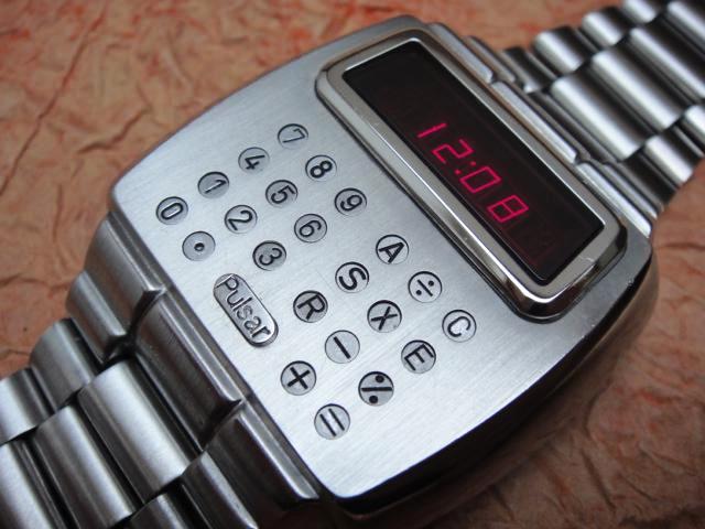 The Pulsar Calculator Watch was the first of its kind and came along with a stylus to operate the miniscule buttons. The circuit board traces would have been laid out by hand, explaining the gentle curves rather than straight lines. The chip-on-board construction is wild, with the silicon die bonded directly to those traces on multiple chips in this image. There is also a mercury tilt sensor on this model that would have switched the display off when not being held up to view the time (or calculate your tip at the Ritz).
We found working models of this watch for sale online for about $225-350. That’s a steal considering the original list price for these is reported to be $550 ($2600 considering inflation).
The beauty of the PCB artwork is hidden away, not just inside the watch case, but obscured by the plastic battery housing to which those tabs on the right are soldered. Think of how many geeks were lucky enough to have one of these and never realized the beauty within. If you’re looking to unlock more of these hidden masterpieces, check out [Greg Charvat’s] article on collecting and restoring digital wristwatches.


What ? no mention of the magnificent HP-01 ?
I was also surprised. The HP-01 was introduced in 1977 two years before this copy.
It was the first non RPN HP calculator.
Inspiring! thanks for sharing!
The circuit board is transparent. I wonder what it was made of? Is it just a slab of epoxy?
It looks like kapton. Much like flex circuits today. This is so leading edge, even today assembly of this is not a walk in the park. Much of the assembly equipment used today for this type of assembly didn’t become mainstream until 15 or 20 years ago.
Probably something like a phenolic resin.
Looks like kynar.
it’s polyamide.
Thanks, this could have gone on forever. This is just another board to an old timer. I remember doing a teflon 5 watt amp board sometime in the 70s and it required 3 artworks due to the various thickness of the material. Plated thru holes had to be sodium etched so the plating had a rough surface.
This makes me wonder how far back SMD components go. That thing is a beaut!
fairchild briefing on integrated circuits was talking about flat pack IC’s (think SOIC but just smaller than a dip) like it was nothing in 1967 for consumer use, and thanks to local favorite Fran we know they were used in the apollo missions
These aren’t really SMD components, they are more like ASICs.
I was referring to the passive components, not the chips themselves :)
They are definitely SMD.. whether they are also ASICs, is irrelevant to that matter.
Not sure what one has to do with the other?
When ICs grew too many pins to fit reasonably in round metal cans, the first rectangular packages were surface-mount flat packs. The Apollo guidance computer was full of ’em. DIPs came later.
Mid 60s, it’s hard to trace before 1970s though, because terminology was all over the place, and some terms were used that mean different things to what they do today. Also the killer apps were all military and aerospace, so they didn’t exactly publish the schematics in Radio World or whatever.
You might have seen oldschool SMD but not recognised it, because it was a single inline module, potted up, on a otherwise through hole board.
Surprising there’s no epoxy blobbing. My first encounter with the black blob was in a calculator. Back in the early 80’s I just happened to have the exact model of a calculator used in a project in a back issue of Popular Electronics. The hack was enabling the memory and constant functions built into the calc but disabled, and adding switches to use them.
But when I opened my calculator, to my surprise inside the pretty bulky white case was almost nothing! Just the display PCB with a single black blob and a PCB with the button matrix connected to the display board. At some point the manufacturer had condensed the entirety of the components into a single chip, but made no change at all on the outside to indicate a different revision. :(
That’s not even the prettiest one! Look at this beauty
http://www.crazywatches.pl/images/upload/led/uranuscalculatorled12.jpg
Indeed thank you for sharing. Back in the day you might lay this up on a 3-ft x 3-ft template using cellophane sheets for your plastic material. Then instead of an enlarger you used a reducer, to shrink it down to that size. Furthermore you really should explain that those are gold wire bonds that lead from the circuit traces to the IC chips. While they still do that technology today It’s hidden from view inside of cases. If you were the bonding operator and you blow any of the IC pads, there is no going back. Today it’s all automated, back then it was purely manually done by skilled grandmothers!
I use Altium designer today for circuit board layouts. They now have an easier automated CAD tool for making curved traces. Gone are the days of giant manual photo resist layouts.
Wikipedia says the first Pulsar came out in 1972, which seems later than I thought, but maybe another company was first.
But, there was a digital watch project on the cover of Popular Electronics about 1974, definitely befkre it switched to a larger format. Wait, it was the Jan 1974 issue. There was a kit, I doubt anyone bought parts and made a circuit board themselves. An LCD readout.
I was aware of the Pulsar, it got a lot of press. But I didn’t pay much attention to digital watches until TI made them cheap, in 1976 or was it 77? But a kit in 1974 seems so early. In that issue of PE they talk about around a million digital watches, and a shortage of crystals to make them.
Not sure of the date, but Hughes Aircrash was building this stuff for contract back in the day and selling them to employees at cost. Still a couple weeks wages, but talk about status until Casio hacked it.
I have a circuit board from a 1970’s hewlett packard test instrument that’s a solid chunk of copper, with depressions milled in it for chips, that were then bonded to the surrounding pads. Like this, all the traces (on a thin sheet of, I dunno, kapton? bonded to the copper?) are curved to where they need to go.
One of my coworkers who uses cadence allegro still lays out her massive test boards this way, all freehand drawing and curves, on 30 layer boards almost half a meter on a side. They’re awful to work on. You get used to tracing routing to find areas quickly, and then using silkscreen to locate individual parts, and somehow it’s much harder on these boards.
Are they just simple breakouts or something? She must be truly an exceptional engineer to be able to do anything like that by hand. I can’t do much of anything technical without CAD of some kind.
For all its clunkiness, at least Eagle CAD allowed you to ’round off’ PCB tracks after you’ve laid them, which can be used to create some more elegant designs.
Because of this article, I just had a look and it seems someone has made a working plugin for this for Kicad https://www.youtube.com/watch?v=ec8EN96jiOc
Going to try this later.
You can do that in Eagle, but it’s something you should do as the last step, because moving around curved traces becomes a total mess.
A lot of pcb designed in Japan using manual layout looked like the layout above.
Curved traces were easier to lay out with the paper tape used for hand layout. In 1975, CAD was the exception, not the rule. Curved traces can often pack more circuitry into small spaces than traces with corners.
SMT components in 1975? Impressive!
Vintage digital watches are absolutely fascinating. Large numbers of microscopic MOSFETs that no watch maker from the 15th century could have ever imagined. Thank you for this interesting post.
Most people today would likewise struggle to conceive a design with all the tiny, intricate parts that make up a purely mechanical timepiece. And they would be just as unable to manufacture them, short of a computer driven machine…
Amazing advancement in technology comparing to the iWatch hardware…Flexible circuit is inspiring
https://www.ifixit.com/Teardown/Apple+Watch+Series+2+Teardown/67385
the link in the article is broken. It should be https://www.crazywatches.pl/pulsar-calculator-time-computer-led-1975