Breadboard CPUs are a fantastic learning experience and require serious dedication and patience. Occasionally, CPU builders eschew their breadboards and fab their design onto a PCB. But this takes away the flexibility and some of the opportunity for learning that breadboard CPUs offer. [c0pperdragon] was doing the same sort of repetitive wiring from project to project as most 8-bit breadboard CPUs use memory, a bus, an IO controller, ROM, and a few other passive components.
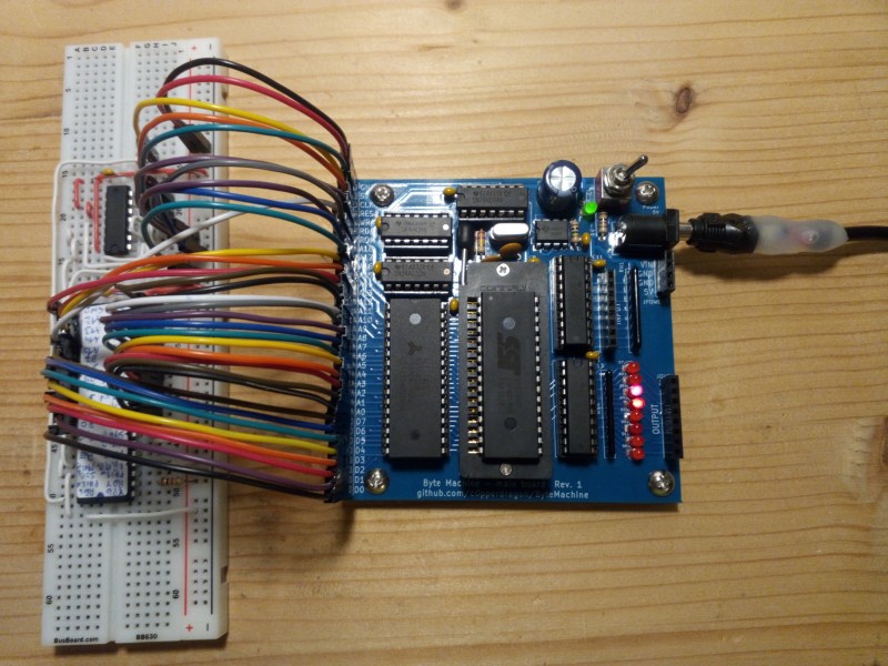
Taking a compromise approach, [c0pperdragon] built a PCB that can be used as a building block in his custom CPUs which they have titled “ByteMachine”. A single row of 34 pins offer power, clock, reset, 19 address bus lines, 8 data bus lines, and a ROM selector. This means that the CPUs can fit on a single breadboard and can run faster as the impedance of the breadboard has less effect on the circuit. With 512 KB of RAM and 512 KB of ROM, in a ZIF socket for easy reprogramming, ByteMachine has plenty of space.
One drawback is the lack of IO. There is no dedicated address space as this would require decoding logic between the RAM and the CPU. [C0pperdragon] added a simple 8-bit output register provided by a 74-series logic IC. The data is displayed on 8 red LEDs and can be accessed via pins. Input is accomplished in a similar way with just 8 bits of digital input provided.
[C0pperdragon] has built the 65C02, 65C816, Z84C00, and the i8088 with the ByteMachine. Each was documented with incredible schematics, pictures, and test programs on GitHub. Next time you’re looking to build a CPU on a breadboard, maybe start with a ByteMachine. In some ways, it might improve your learning experience as it makes the incredible mass of wires we’ve seen on other projects a tad more manageable.
Thanks [Reinhard Grafl] for sending this one in!


https://www.grammar-monster.com/lessons/abbreviations_forming_plurals.htm
Confusing, but HAD titles are always ALL CAPS.
Not just confusing, but often entertaining!
I hear this a lot. Some say that breadboards are only good for up to 1MHz to 5MHz.
I’ve run 40+MHz digital circuits on breadboard.
Some sensible design and lots of bypass caps and your good to go. Though it helps that I have a background on analog RF.
It’s useful for design phase but just putting your hand near the board when it’s running will cause a crash.
I did one 50MHz VGA output generator on a breadboard. Putting a finger on the SRAM chip randomizes the memory – useful for testing.
And I flung a BB with a popsicle stick
Oh, you’ve hit the credibility wall, right there.
Solderless bread boards are indeed a wonderful learning opportunity
You learn the effects of random varying conductor resistance, capacitance between conductors, inductance of wires, ground bounce, and signal integrity in general.
After you have learned all that, you can begin to concentrate on your design.
You do well to keep the clock rate within sensible limits, that is for sure.
So, the CPU being developed/tested is on the breadboard, and the ByteMonster is connecting to the breadboard.
Now, is the chip in the ZIF required? Or only for programming something?
And why 34 connections if most 8-bit CPUs have 40 pins?
>>And why 34 connections if most 8-bit CPUs have 40 pins?
Because it has enough pins to expose the functionality of the ByteMoster to the CPU, not the other way around.
A “commmon denominator” of RAM, ROM, CLOCK, RESET and a single input and output I/O port
Anything beyond that, custom to your partcular CPU, you put on the breadboard.
>>Now, is the chip in the ZIF required? Or only for programming something?
That is the ROM.
ZIF because you will be pulling it out frequently to put in your EPROM programmer.
Not me man. I use my EPROM emulator, leave it plugged in for the entire development cycle, then burn a final EPROM when I am all done.
I do remember those days where running out of erased eproms stalled testing. Never again.
Clock frequency/period is completely and utterly irrelevant. The only parameter that matters is the rise/fall time.
If you want be anthropomorphic, realise that when a transition occurs the circuit does not know nor care when the next transition occurs.
Any setup and hold time violation is a problem whether it occurs once per second or a million times per second. Ditto an invalid voltage which may causing incorrect operation.
You seem to know the right words, so it’s hard to imagine how you can be so wrong about this. The simple fact is, once you meet all of the setup and hold times, this dictates the clock period, because that is the point where you can’t reduce the setup and/or hold times any further, and at this point you have found the minimum clock period. In fact, in most cases, the numbers add up pretty closely. Grab any MPU datasheet and show me a case where you can go significantly faster than the max clock speed without violating a setup or hold spec. I don’t think you’ll find such a case.
Not everything is related to the “main” clock; there can be other clocks at different frequencies and/or phases. The setup/hold time is relative to the relevant clock.
That is very definitely true in many (most?) FPGA designs, and it is even true in some MCU systems. For example, with the XMOS xCORE processors it is quite normal to choose differing clock frequencies for different I/O ports, and also for different processor cores.
Yes, so apply what I said to any given clock spec. Your reply is non-responsive, and in no way backs up your original claim.
You’re both raising valid points but there is much more to designing high (clock) speed circuits on a breadboard.
Firstly, on a PCB you usually have a large ground pour so when you connect to ground anywhere on the PCB then you can be reasonably confident that the is the same ground reference as any of the chips.
However, a breadboard layout works with what is effectively an balanced power supply (rather than an unbalanced of ground referenced power supply) so ground potential can (and is often) different in various places on the breadboard. This is especially true with regard to AC signals such as high clock speeds causing transient spikes. DC differences in ground potential should be relatively very low.
Rise (tr) and fall (tf) times have been mentioned and this is a function of slew rate due to stray capacitance in the case of breadboards. However there is a significant difference. (tr) is simply the time it takes a signal (Vs) to rise to Vih and (tf) is the time it takes (Vs) to fall to Vil. But what does that mean when (Vs) is referenced to the ground pin of source chips and Vil and Vih are referenced to the ground pin of different chips which may have a different (AC) ground potential.
So immediately you cans see that there may be different issues with different IC technologies. For exampled there are more complex issues to deal with for technologies with asymmetric output drive currents like TTL when compared to NMOS or CMOS.
There are ways to mitigate these problems to allow you to achieve higher frequencies and some of them may seem counter-intuitive.
First is the obvious ones –
Put bypass caps directly across the Vcc-GND pins of the chips.
Run every Vcc / Ground pin to the bus rails on the edge of the board using equal length wires. Definitely don’t daisy-chain Vcc or GND around the board.
On a standard breadboard (size) place a 100nF and a 1uF cap on both sides of the edge power rails where you have to link across the middle of these rails. Use the shortest possible wire here.
Place the same 100nF and 1uF combination where the external PSU connects to the rails.
Don’t use all four rails, just use 2 either above or below.
Use pull up or pull down resistors instead of direct Vcc / GND connections for unused inputs. Definitely don’t leave unused inputs NC.
Connect the external PSU to the left of the board. Place the Vreg first on the left if you have a onboard Vreg. Then place the highest clock components next. Then the lower frequency signals as much as possible going from highest frequency to lowest from left to right.
The less intuitive things are –
A transient current spike is (and the resulting voltage spike) is not just a function of frequency but of course also a function of current.
If you have a higher current high frequency device like perhaps a crystal oscillator block then it may well pay to place very low value resistors in the Vcc and GND lines. Less intuitively it may be better to limit current by placing a series resistor in the output line. Yes, this will decrease slew rate and increase tr and tf but that doesn’t matter because they will both be the same period anyway and unless the resistor is to high they will still be symmetric to the larger degree with with asymmetric technologies.
The less obvious thing here is that even though there is little change in the clock signal to the next stage … the likelihood of issues in much lower frequency parts of the circuit is greatly lower as there are far lower transients being injected into the power rails.
Thank you for pointing out many of the concerns whenever designing high-speed circuits, but I was really only responding to the claim that as long as you get your rise and fall times right, the clock frequency doesn’t matter, rather to the whole gamut of digital circuit design and layout.
Having designed a number of commercial single-board computers and high speed test fixtures, I can assure you I would never use the so-called “breadboards” that are so popular today for such things. I tried once, with a microcontroller I thought wouldn’t be too finicky. I ended up moving the chips to a proper breadboard, which to me means copper-clad with manhattan/deadbug style wiring. Which doesn’t take much longer to throw together, and doesn’t stop working when you move your hand towards it.
So, you’re comparing CPUs implemented with 74-series logic chips with one that is just a matter of an “everything but the CPU” PCB with only the CPU itself (and maybe a clock generator) on a breadboard. Great.
I mean, it IS a good idea, separating the peripherals from the CPU, and one that was done a lot in the 1980s, with the S-100 bus, Intel’s Multibus, and later on, conventions like PC-104 and just last week, RC2014. But putting the CPU on a breadboard? That just seems backward.
There also was ECB, which was based on the once popular Europa Card format (100x160mm). :)
https://www.elzet80.de/ecb.html
I’ve got a couple of Heath ET-3400s and I’ve been wanting to make something like them. This project is sort of the other way around, more like an Arduino-ish CPU board but with pins only down one side. I’m still not sure whether it’s a module for the breadboard or the breadboard is a module for the CPU board.
What I usually do (and just set up another one today) is stick a Blue Pill into a breadboard. It makes for a tidier build if I can use .1″ headers right on the GPIO pins. Never underestimate what you can do with ribbon cables! Right now I’m working on a 5-octave keyboard I got in a junked cheap synth, but the it has full diodes, and two 8-wire cables, perfect to hook up to an MCU.
But that’s only one kind of CPU, though my Blue Pills are only two bucks each, and I bought a bag of them a while back. I’ve also been trying to put together simple blocks like a row of LEDs driven by SOT-23 transistors.
Unfortunately for my ET-3400 clone idea, those little mini breadboard blocks are either not cheap or not available, but female pin headers are plentiful, both single and double row. Keypads wouldn’t be too hard with Cherry switches, and clones with the [+] tops can take key caps from a particular era of bad Apple rubber dome keyboards. (Unfortunately someone decided long ago that the pins should be 0.1″ by 0.25″ spacing, so it they won’t fit in breadboards or hole grid boards.) Eventually I’ll get back to doing PC boards again. At least I’ve gotten all my old Eagle stuff into KiCad.
It would be much more versatile if you placed a small CPLD between the CPU and SRAM/FLASH. Something like the Altera EPM240 / EPM570 which is 5v tolerant with series resistors (seems to work fine without them), or the Xilinx xc9536xl / xc9572xl which is directly 5v tolerant but has Vcc 3v3. Running them at 3v6 gives better noise margins.