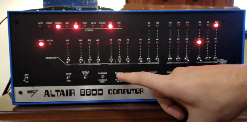
If you aren’t old enough to remember when computers had front panels, as [Patrick Jackson] found out after he built a replica Altair 8800, their operation can be a bit inscrutable. After figuring it out he made a pair of videos showing the basics, and then progressing to a program to add two numbers.
Even when the Altair was new, the days of front panels were numbered. Cheap terminals were on their way and MITS soon released a “turnkey” system that didn’t have a front panel. But anyone who had used a minicomputer from the late 1960s or early 1970s really thought you needed a front panel.
You may never program an Altair by the front panel, but it is still an interesting glimpse into what computing looked like only a few decades ago. While you might think that the front panel was a mere curiosity, it was not unusual to have to key in a bootloader program manually so you could then load other software — often a better bootloader — from paper or magnetic tape. Some computers even had the early bootloader code printed on the front panel for reference.
A front panel can also help you debug programs and hardware problems since you are probably looking right at the bus in a real computer. Of course, with an emulator, the emulator is just driving the front panel for make-believe, but it still works the same way.
We did our own front panel tutorial for the PDP/8. The operation is similar, but not exactly the same. The front panel for the BLUE computer was especially fun because it used the limited lights and switches available to the FPGA board it lived on. You can see it in a video in this post about the real-world implementation of a fake educational computer.


The thing that actually did away with front panels wasn’t terminals, it was cheap and easily programmed EPROMs.
Most scratch-built computers had some form of keyboard and display, whether these involved a surplus terminal of some sort, or a built-in video generator and an I/O port that could scan a keyboard switch array, or even just a numeric keypad and a hexadecimal 7-segment display. Otherwise, what were we going to be able to DO with them?
On my first computer, I used switches for address and more switches plus LEDs for data, along with write, reset, and interrupt switches, which I used to enter and debug programs, having no way to store programs, not even EPROM. Ask me about snow crashes. On my second system, I included an EPROM socket, and a “front panel” with an SRAM chip that could plug into that socket to emulate the EPROM, until I had a working monitor program I could burn into an EPROM. Once I had that, I modified the EPROM emulator to make it into an EPROM programmer. This is what “bootstrapping” really was about – developing a system step-by-step to make it more and more useful and convenient. This monitor program, which then ran every time the computer started, then allowed me to type in programs instead of flipping switches, and battery-backed SRAM allowed me to keep programs from one session to the next, because persistent storage (tape or floppy disk) was still another big step away. But it was that EPROM monitor that eliminated the need for blinkenlights. Terminals weren’t even a factor, since the computer contained all of the pieces that a terminal could have done, and a terminal was of no use until you had some way of getting a program into the computer.
I was very lucky that I didn’t make enough money to buy something like an Imsai or Altair, because I got to experience this whole process, bumbling my way from one step to the next.
I remember using a microprocessor trainer in the early 80’s that had an EPROM monitor and hex keypad. At the time it felt like bare metal programming, but now I understand how much of a boost that monitor program gave me.
Yes, the Altair launched, and very rapidly the front panel disappeared.
That front panel was needed right at that point, but the success meant others followed and better schemes.
Once you had an eprom, or maybe it was a better sense of what these home computers were going to be used for, the front panel became a liability. A lot of discrete circuitry, adding to the cost and complexity, and then mostly “thrown” away after a brief use. It had to put data from the switches directly ito RAM.
A monitor in ROM was more versatile, and worked with a serial terminal or a simple keyboard and readout, the CPU doing the work.
When introduced, the KIM-1 was “cheap” but comparable to the basic Altair (though no motherboard to plug in expansion boards). Using a monitor in n ROM made for the lower pricing.
A friend and I put together a KIM-1 and a power supply in a hotel room in Denver after buying the KIM at the computer show and the power supply kit and soldering iron at a local Radio Shack. I still have it.
I got a SYM-1 from my coworker. Works great, and I’m making modern rom chip options for it.
What about diode matrixes?
This was before my time, but I read they were used in morse keyers for beacons, amateur radio repeaters etc.
So I wonder if they ever were used to store IPLs or tiny monitor programs also..
Somebody else here mentioned diode matrices for ROM, but I never considered that because of the sheer amount of wiring that would have required for any significant piece of software. An average of four diodes would be needed for each byte, in addition to the logic needed to select the desired byte. WAY too much work. I DID use a diode matrix to encode my keyboard though, which allowed it to send 7 bits of parallel ASCII to an input port in the computer. With no keys pressed, that port would read as 0000000, and each key had a diode for every “1” bit in its code. The monitor program polled that input port about 20 times per second, and any value other than 0 indicated a key had been pressed. This was not able to do any roll-over, that is, if more than one key was pressed, it would give the logical OR of the two codes. To avoid wrong codes, the keyboard reading subroutine, once it detected a key press, would ignore any other keypresses until it read a code of all zeros again, indicating that all keys had been released. Which was rather crude, but I learned to type on it reliably.
The closest I got was a diode decoder for lower-case on a TRS-80 Model I that had a character generator chip without descenders. If it decoded any of gjpqy,; (using the diodes as a primitive PLA) it would cause a 7483 to subtract two from the incoming row number. That 7483 ran a little warm, yeah.
I am considering making a little diode matrix module if I get around to doing one of those bare-bones computer on a breadboard projects. I already have a few 2×20 female PCB-mount headers set aside for the project. Four LS138 chips would decode 32 bytes, plenty for a boot loader, or a simple LED blinky program. It’s cooler than using a 2864.
Huh. I know I studied the Model 1 schematic, but I had forgotten this part! Thanks for that.
In my own first computer, I wanted to be able to do graphics better than the Model 1’s clunky “graphids” mode, so I designed the display to use a RAM character generator, which in graphics mode gave pixel-level addressing, which was initialized for standard ASCII character generation, allowing both fast character drawing and also “high resolution” graphics. But at that point I had not yet discovered how easy EPROMS could make things. There was a chip, the General Instrument RO-3-2513, which was a mask ROM preprogrammed with 5×7 dot matrix characters. Which is I think what the Model 1 used, and which was upper-case only, and had no descenders. There was a companion chip, added a little later by GI, that did lower-case characters. But the descenders had not been anticipated, and used just as they were, these chips would produce text that had the lower-case letters offset one pixel up from the upper-case ones. Some low-cost terminals just used these as-is, which I thought was unnecessarily ugly. This is what Tandy’s clever adder chip did on the fly as the screen was refreshed. My solution to this quirk of GI’s character generators was to shift the lower-case characters down one line when copying them from the ROM to the character generator RAM.
But no, I never would have tried to do a whole character generator ROM with diodes!
TRS-80 Model I used a 128-character Motorola chargen that had lowercase, but some versions of the chip had those seven descenders raised into the full seven rows. And it was an 0.3″ narrow DIP. The adder was just my own circuit to correct for that version of the chip.
The 2513 was half as many bits (64 characters), on an 0.6″ wide DIP. It also required the funny voltages of old ROM chips. The ADM-3A was famous for using that.
Sorry, I misunderstood – I thought you were saying that Tandy did this. This explains why I didn’t remember that. Nice hack.
I’m looking at the 1977 GI catalog pages for the RO-3-2513, though, and you’re wrong – it’s 5V only. I KNEW I didn’t have +12 and -5 in my machine, so I was wondering how I did it, since I distinctly remember having to fix the descender problem, which as I said, I chose to do in software. The -001 was the upper-case chip, and the -005 was lower-case (vertically shifted up by one row) and some special characters, which took the place of what would have been ASCII control characters. But even THAT they got wrong – you had to invert ASCII bit 6 for the characters to decode properly. Again, fixed in software.
The Signetics 2513 data sheet shows -5 and -12, so your GI version was probably later.
Also for some reason the ADM-3A used a 2513 with inverted character code inputs for lower case. So they just used both the Q and Q! outputs from the character code latch. Bit 6 was used as OE! for both chips. The lowercase characters were tiny and raised above the baseline. It looks a bit odd.
I understand – in the memory business, there were many chips that shared the last four digits of their part numbers, with the prefixes telling whether they were erasable or not, and other variations. Most of the ads said either “5V only” or “5,12,-5V”, just to avoid misunderstandings. I am specifically calling out the RO-3-2513, which was a hot seller in mail-order sales in 1978, which was when it became practical for me to build a computer, using a Z-80A (~$50 from Jameco, as I recall), those character generator ROMS, Intel 2101 SRAMs ($1 each * 48), and 74LS logic for everything else (roughly 16 chips at < $1 average). Wozniak would have snorted at my choice of SRAM rather than DRAM for system memory, but with very little available to me in the form of instrumentation and little hands-on experience with digital logic circuitry, I was more interested in success than large memory capacity. As it happened, I built my next system before I ever wrote anything that needed more than the 6 kB the first machine had, so I consider my choice to have been a good one.
The ADM-3A was specifically designed to be a low-cost terminal, and took shortcuts like this. Having used Datapoint 2200 and Tektronix 4012 terminals, I had slightly higher standards. As I’ve already said, GI clearly wasn’t thinking ahead when they designed the programming for the RO-3-2513-001, or they would have left the bottom row of pixels blank rather than the top row, to allow it to work seamlessly with the -005 lower-case ROM.
Sure, you could use _your_ 2513 with no -5 or +12, because you only had one of them and knew what you had. If you were using thousands of them, your choice was either hook up those power supplies or be limited to only some of the suppliers. If the Signetics was 50 cents cheaper, too bad. And in 1977 there may not even have been a single-supply 2513, with other devices needing them too. Later as those other voltages became unnecessary, the cost of those power supplies for just one chip was too much. That was a time when there was a lot of change in which process to use, even one year made a difference. But you couldn’t simply put your product on the shelf for a year just in case they got rid of those voltages.
Also GI may not have designed those pixels, they probably copied it from the existing documented design.
If you blindly ordered a 2513 without the full part number, nor even the assurance that it was a 5V part, you would likely not have gotten what you wanted. And for that matter, a 2513 was a generic number for a mask-programmed ROM. You had to know the manufacturer and suffix in order to know what MASK it used. With EPROMs, there were parts that required 25V for programming, and others 12V. In the 1977-80 period, there was a big transition going on from PMOS to NMOS, with PMOS requiring 3 supplies, so you definitely had to pay attention to this sort of thing. NO manufacturer produced PMOS and NMOS parts without making a distinction between them. But if you ordered an RO-3-2513/CGR-001, you knew what you were getting, because this was fully specified and unambiguous part number. The “back of the magazine” advertisers were well aware of this, which is why, even when they gave the full part number, they almost always also gave the “gotchas”, like power supplies and speed rating. I think it was common to sell character generator ROMs as “AY-3-2513”, because “AY” was a General Instrument prefix. But according to GI, that wasn’t a valid part number. Sort of like calling the Messerschmitt BF-109 an ME-109, or a DE-9 connector a DB-9 — everybody would know what you were talking about, but it was technically wrong. I stayed away from those vendors, because if they were being sloppy about part numbers, how could I know what I was buying? So yeah, I probably DID pay a buck more for my CG ROMs than I strictly had to.
Also, as I’ve already said, the datasheet I’m looking at was from GI’s 1977 catalog, and they were available then. I bought mine in 1978 in the surplus market. Sure, Signetics made a PMOS version, but this was a generic masked ROM, but it was certainly worth my while to look for the GI part.
You would need far to many diodes for that sort of thing. You’d be looking at hundreds or thousands. However, there were equivalents in some ICs. Fuseable link memory comes to mind. I used to program answer back boards for Texas Instrument Silent 700 terminals. Those were 21 characters times 7 (IIRC) diodes.
Diode matrix memory would have been feasible as a hobbyist solution for up to 32 bytes or when EPROMs weren’t affordable, just enough for a simple bootstrap loader.
Certainly. There was a window in time, when diode matrices would have been the method of choice for storing boot code, at least. But we’re talking about a short window, from when microprocessors became available and affordable, until EPROMs became available and affordable.
As I mentioned in a different thread in these comments, I know that DEC offered diode matrix boot ROM modules for some of their minicomputers, as an alternative to the full front panel, primarily for users who weren’t developing their own low-level code, and wouldn’t benefit from the diagnostic uses for the front panel. But this was before the microprocessor, when few hobbyists were building computers.
What I’m surprised by, is that even though I see people making CPUs out of discrete transistors or even relays, I don’t see a lot of those people using diode matrix ROM in those systems. Or ferrite core rope memory, for that matter (the type of ROM used in the Apollo Guidance Computer).
He goes into great detail about what octal IS, but doesn’t mention WHY it was used on the Altair, and other 8080-based computers. The separation of the 8-bit instruction word into three fields, 2 bits + 3 bits + 3 bits, happened to be how the instructions were actually encoded for most of the 8080 instructions, where the first two bits were the op code, the next three bits were one of the operands, and the final three bits were the other operand. (There’s more to it than that, but basically all of the instructions fit nicely into these three fields.) This allowed users to quickly recognize what the instructions were, just by looking at the lights. This also worked for Z-80 based machines, since these were backward-compatible with the 8080.
That was a convenience of using octal, but octal was used for representing values in computing long before the 8080 existed.
Ever wonder why UNIX permissions are in octal? Ever notice that the PDP-8 switches are colored in groups of three? Or IBM 360?
When I worked at NCR in the 80’s and 99’s several of the ECR”s were programed in Octal because they used the MED-80 processor chip (a cousin to the 8080). However to set options in the program the data was in first configured in 8 bit BCD that was converted to Octal before the programmer (me) keyed it into the register. The feature program ( which included the name of the grocery store )was keyed into and stored in NVRAM while the base program ( control of totals, reports, etc.) were in EAROM.
I recently typed in a scan of an H19 ROM assembly listing and made it assemble to generate the proper binary code, to confirm that I typed it in correctly. The thing that surprised me was apparently Heath’s assembler had a type “A” constant which was two three-digit octal numbers, because apparently that’s how the H89 front panel displayed addresses. So instead of 177777Q they would use 377377A for address 0FFFFH. But I was always a Z80 guy, and even though I understood why, I never liked the idea of using octal.
On the other hand, most of the 68000 opcodes were broken up into 4-3-3-3-3 bits like the PDP-11, but I never heard of anyone using octal with it.
The PDP-11s that had switch panels (not all models did) used color-coded rocker switches that were in groups of 3, but in the 1-3-3-3-3-3 bit pattern, not the bit pattern you describe for the H19! I don’t think I’ve ever seen a 68000 system that used a switch panel. I attribute this to the almost universal use of EPROMs for boot code by the time these systems were introduced. I do recall that at least some of the DEC minis had a boot ROM option, that was expensive and small because it was implemented as a diode matrix with soldered jumpers for each bit.
It’s possible to write a simple tape based bootloader in as little as around 40 bytes in 8080 code (which isn’t too impractical to toggle in (though I may find leading spaces have been removed when I post this, making it hard to read)).
Strt:
21 00 01 lxi h,100h
11 00 00 lxi d,0 ;e=prev bit, d=chk.
NuByt:
3e 80 mvi a,80h
NuBit:
47 mov b,a
0e 40 mvi c,40h
BitLp:
db fe in Cass ;b7
ab xra e
fa 15 00 jm zcross
0c inr c
c2 0b 00 jnz BitLp:
zcross:
;80..bf=0, c0..ff=1
79 mov a,c
87 add a
d2 00 00 jnc Strt
8f adc a ;bit=>cy
78 mov a,b
1f rar ;
d3 08 00 jnc NuBit
77 mov m,a
23 inx h
82 add d
57 mov d,a
77 mov m,a
c3 06 00 jmp NuByt ;40b.
It uses a zero-crossing technique where 0x60 BitLp cycles == a zero and 0xa0 BitLp cycles == a one. On a 2MHz 8080 this is 3744 cycles for a zero and 6240 cycles for a one, equivalent to 4992 cycles per bit on average or about 400 bits/s, fairly typical for early cassette routines.
the routine jumps back to the start whenever it finds an invalid bit; thus the end of a program on tape should cause a jump back to the start. It also implements a checksum: the byte after the last byte of the program contains the sum, so starting a tape; pressing pause when the tape goes silent after the program, then checking the expected checksum address should let you know if it’s been loaded. Because it uses no subroutines and holds all variables in registers, all the remaining RAM is available for storing programs.
Bootstrapping such a system could proceed as follows:
1. Write the tape saving routine (probably another 40-odd bytes).
2. Use (1) to save it to tape.
3. Write the tape loading routine above.
4. Use it to load the tape saving routine. Now you can toggle in new programs and save them.
5. Turn the tape loader (now it works) into a ROM. The simplest, given we don’t yet have an EPROM programmer is to implement it as a diode matrix. This program has 115 bits set, which needs 115 diodes if we invert the outputs.
There’s always some trade-off between developing tools to make programming easier and actually writing programs to solve real problems. Toggling in programs is still very laborious, so I guess the next steps are to write a trivial hex-pad based monitor in the order of 256 bytes or so. This would improve productivity by a factor of 4 or so.
I don’t have the code at my fingertips, but I assure you, the keyboard based monitor I wrote was not much longer than your bootloader. And like I said earlier, it was the ease with which I could build an EPROM programmer for the 2716 that made the front panel obsolete.
Bill Gates has you beat by 27 bytes, and Josh Bensadon by 28 :-) https://hackaday.com/2017/03/24/doing-it-with-fewer-bytes-than-bill-gates/
From what I can tell, the Bill Gates loader was for paper tape. This one is for cassette, which is much more interesting and easier to make tapes for. Cassette tape players were plentiful and cheap, unlike paper tape punches. Also Z80 would save 4 or 5 bytes just from using JR instructions.
This would depend, to a great extent, on what you were using as the primary I/O device. There were a lot of Teletype model ASR-33s out there, and if that was what you were using, you already had a paper tape punch and reader.
This reminds me of some of the early digital pbxs that I had to program with toggle switches in hexadecimal they used input load and run switch positions and kept permanent memory in a dc300 cassette twice as large as the usual audio cassette.
I’d like to see something about the Altair 680. I built and operated an IMSAI 8080 growing up so I understand how that front panel works. But the 680 doesn’t seem to have a deposit next switch so I’m trying to figure out if you had to put in the entire address each time with the data byte and then hit deposit? Anyone?
Yup, I think you need to change the address manually for each byte. The MIT 680’s front panel is considerably simpler than the 8080’s and doesn’t have address auto-increment. See this webpage for the MITS 680 schematics and manuals, particularly the operator manual: https://www.vintagecomputer.net/MITS/680/index.cfm
But notice that the Altair 680 had separate rows of switches for address and data, while the 8800 saved a few bucks on switches by sharing them for address and data. So on the 680 you just had to change from the current address to the next address, rather than setting the full address. You get the pattern of incrementing binary into muscle memory pretty quickly – I like this arrangement better than the shared switches + “deposit next” and “examine next” switches, and it’s a lot simpler to implement. You also see the address on the switches, making it easier to verify that you haven’t skipped an entry, while the “deposit next” panels you had to wait until you had deposited a word to see what address it got deposited to on the address LEDs, which seemed unnatural to me. Some front panels (like mine) used either octal or hexadecimal thumbwheel switches for address, making this even easier. You just had to remember to carry after 7 or F.
My first computer was an IMSAI 8080, which was a better quality Altair clone. Also, many years ago, I was a computer tech, maintaining computers such as Data General Nova & Eclipse, DEC PDP-8, PDP-11 & VAX 11/780 and others. Most of those computers had a front panel.
Yooo, I’m the guy who made those videos. Guess I got to make more!
Had no idea there was still an interest in this.
Thanks! I never owned an Altair or IMSAI, but did use other computers with front panel address and data switches, some of which used the “deposit/deposit next” method of incrementing the address.
I don’t know how many people will use your video to help them with their dusted-off hardware, but as you can see from the comments, you’ve lit up a whole lot of neurons that haven’t been used in a long, long time.
Well, that many that are hobbysts about old computers and buy or create emulators of them :) …at least
Front panels on minicomputers survived well into the 90s, albeit with reduced function.
I was sysadmin for an IBM System/36 around the mid 80s – scroll down here to see the front panel:
http://www.corestore.org/36.htm
It was early in my career so I didn’t play around with it, but I was shown by an IBM CSR how to code a “fast IPL” on the panel – it bypassed a lot of hardware checks. From what I remember, there were functions to step through CPU instructions and view register contents.
Then when we upgraded to as AS400 in the late 80s, it still had a service panel – a separate service processor where you could select a few maintenance functions – normal IPL, IPL from “B” copy microcode (where the “A” copy needed an upgrade), boot from tape instead of disk (major OS upgrades), and some other debug/maintenance functions, such as “display last error code” and so on. The list of functions went into double digits, so it wasn’t simply a couple of options.
Front panel, yes, but not a programming panel, which we’re really talking about here – from what I can see, you can’t read or write specific memory locations from it.
And here’s some info on using the System/36 front panel to extract the MASTER account (“root”) password:
https://groups.google.com/forum/#!topic/comp.sys.ibm.sys3x.misc/Vi57cbw1ofQ
Not at that time. There might be many old systems already hacked, but not quite exactly in their time of glory.
My first “personal computer” was the Radio Electronics Mark 8 that used an older Intel 8008 (before the 8080). It had a 14 bit address bus and the upper two bits of what would become the 15th and 16th address bits on an 8080 were used to decode bus cycle types. The original front panel for the Mark-8 decoded these two bits into 4 states (I forget their exact meaning). I used paddle switches instead of more expensive toggle switches. All of my TTL support chips were equipment pulls I got cheap from a place called Poly Pak in Lynnfield, MA (there were a lot of surplus stores in that town).
The Mark-8 used a series of 4 synchronous binary counters for simulating the addresses. You’d enter the address on the binary switches, hit the “latch” button to load that address into the counters, then start entering the 8 bit data and press the “store” button when done. That would generate a single memory write cycle and then advance the address counters to the next sequential address for the next byte entry. I got real tired of that, so I made a simple 7-segment hex display with hex keypad for entry, which worked great and save me a lot of time later.
My Mark-8 was used for my senior design project in college which was a 1702A UVEPROM programmer I redesigned from an Intel app note since I couldn’t afford or get many of the parts they listed. The 1702A was 256 by 8 bits (big wow back then!) and since it was PMOS, it used +5 and -12V supplies. When programming, the -12 was pushed to -46V for the programming pulse. I sweat a lot when I tried this the first time since I was doing this blind (no scope but I did have an EICO kit FET-DVM). Of course, I verified the programming pulses without the expensive (about $25 each back then) 1702A in place.
Conveniently, I could key in my program along with the 256 bytes to program into my (also home-made) 2KB SRAM board populated with sixteen 2102 1024×1 chips, and then single step the program once it was entered and reset (the above counters also served as the processor address latch). This let me statically test that my program and hardware was working. I spent hours upon hours doing all this back in late 1976 through early 1977. I did (finally) get an A for my effort.
I ended up giving that “PC” to a friend at work to use to get the rebate for a Commodore 64. I should have kept it for sentimental reasons.