[SM6VFZ] designed, built and tested a switched-mode DC-DC boost regulator using the core independent peripherals (CIP) of an ATtiny214 micro-controller as a proof of concept, and it looks pretty promising!
A Buck, Boost, or Buck-Boost switching regulator topology usually consists of a diode, a switching element (MOSFET) and an energy storage device (inductor/capacitor) in the power path, and a controller that can measure the output voltage, control the switching element and add safety features such as current limiting and temperature shutdown. A search for switching regulators or controllers throws up thousands of parts, and it’s possible to select one specifically well suited for any desired application. Even so, the ability to use the micro-controller itself as the regulator can have several use cases. Such an implementation allows for a software configurable switch-mode regulator and easy topology changes (boost, buck, fly back etc.).
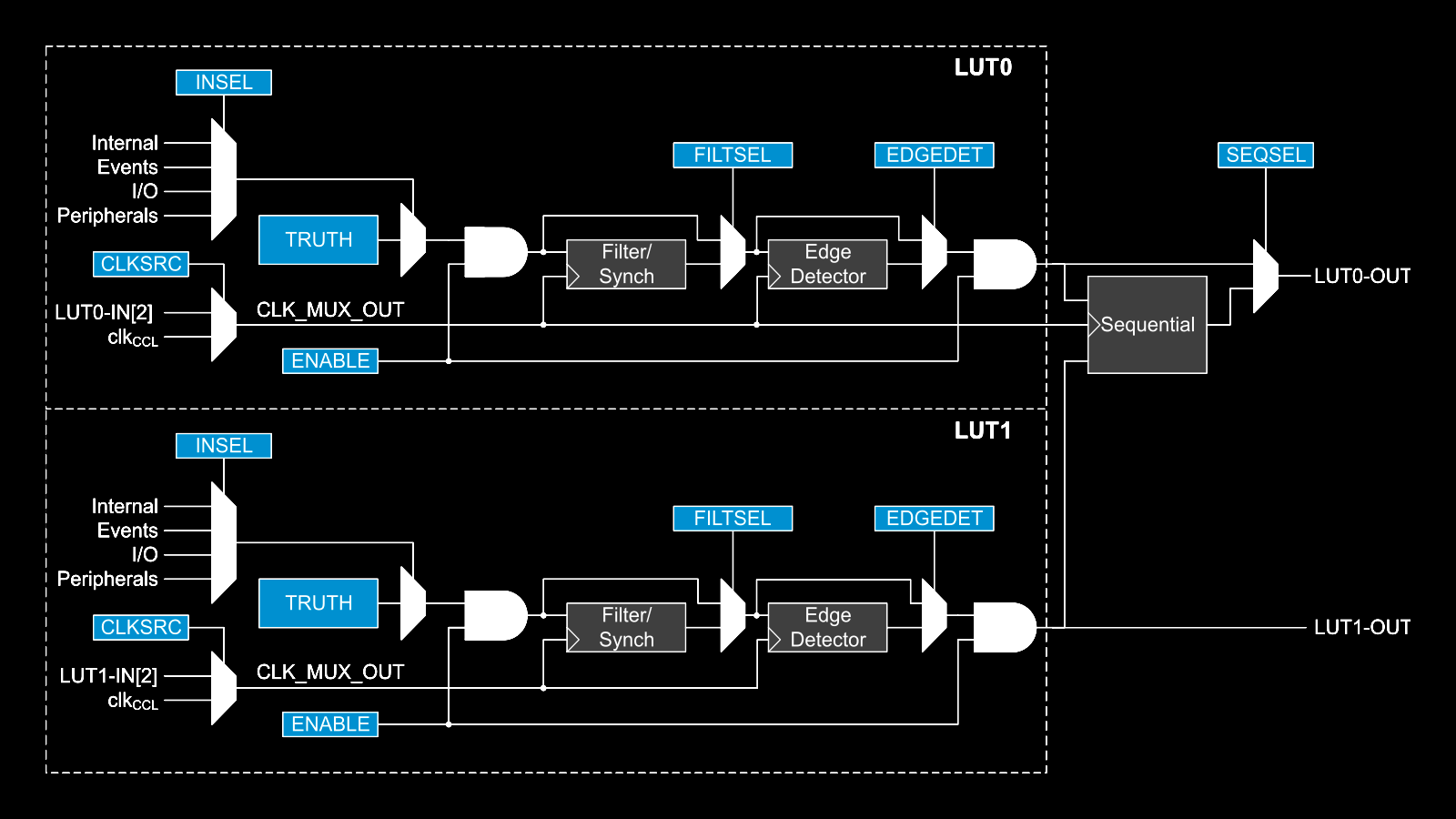
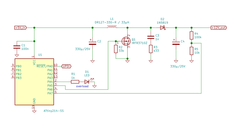
The “Getting Started with Core Independent Peripherals on AVR®” application note is a good place to get an overview of how the CIP functionality works. Configurable Custom Logic (CCL) is among one of the powerful CIP peripherals. Think of CCL as a rudimentary CPLD — a programmable logic peripheral, which can be connected to a wide range of internal and external inputs such as device pins, events, or other internal peripherals. The CCL can serve as “glue logic” between the device peripherals and external devices. The CCL peripheral offers two LookUp Tables (LUT). Each LUT consists of three inputs, a truth table, a synchronizer, a filter, and an edge detector. Each LUT can generate an output as a user programmable logic expression with three inputs and any device that have CCL peripherals will have a minimum of two LUTs available.
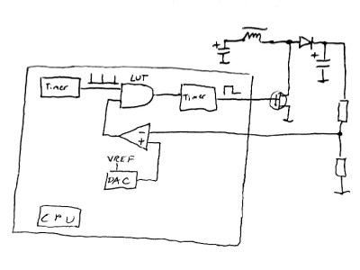 This napkinCAD sketch shows how [SM6VFZ] implemented the boost regulator in the ATtiny214. The AND gate is formed using one of the CCL LUT’s. The first “timer 1” on the left, connected to one input of the AND gate, is free running and set at 33 kHz. The analog comparator compares the boosted output voltage against an internally generated reference voltage derived from the DAC. The output of the comparator then “gates” timer 1 signal to trigger the second “timer 2” — which is a mono-shot timer set to max out at 15 us. This makes sure there is enough time left for the inductor to completely release its energy before the next cycle starts. You can check out the code that [SM6VFZ] used to built this prototype, and his generous amounts of commenting makes it easy to figure out how it works.
Based on this design, the prototype that he built delivers 12 V at about 200 mA with an 85% efficiency, which compares pretty well against regular switching regulators. Keep in mind that this is more of a proof-of-concept (that actually works), and there is a lot of scope for improvement in terms of noise, efficiency and other parameters, so everyone’s comments are welcome.
In an earlier blog post, we looked at how ATmegas with Programmable Logic came about with this feature that is usually found in PIC micro-controllers, thanks to Microchip’s acquisition of Atmel a few years back. But we haven’t seen any practical example of the CCL peripheral in an Atmel chip up until now.


Not to dampen anyone’s parade, but most of the PIC micro [and I assume other] programmers do this. A useful circuit idea anyway.
Dang, missed reading all the article, sorry.
Another area you could explore with this is synchronous switchers, which use another fet in place of the diode. They can get efficiencies into the 98% area across much of the v/i space, and are an area of continuing research as correctly timing the gate pulses to avoid shoot-through while optimizing fast switching is non-trivial.
Hmmm, there’s an itch in my brain saying NASA published some stuff on those.
A bunch of people are doing work with them, and there are plenty of commercial examples. (I’m characterizing one at work right now.) But it’s also an area that’s interesting to play with on your own if you want. A synchronous Ćuk converter with a coupled inductor would be a really interesting challenge: it’ll buck or boost at very high efficiencies with very low radiated emi.
if you want a challenge – bidirectional converters. If you still need more punishment – bidirectional AND buck or boost.
You’re in luck then. Such a thing exists (including coupled inductors, Wurth makes those). Check out the LT8710: https://www.analog.com/en/products/lt8710.html. LT8714 is also pretty cool. You can make a switching, 4 quadrant supply pretty easily with it.
Hey, the CCL is a cool resource to build decoders to protocols like manchester or as address decoders to interface with microprocessors (Z80, 6502, etc).
I think a lot more interesting would be a microprocessor AS a complete SMPS: https://www.romanblack.com/smps/pic-smps.htm
The push-pull GPIO is abused and no additional FET is needed. Worthy of a Hackaday article on its own.
+1 on synchronous converter. It is a shame to use a diode if you have whole micro at your service. In fact a full MOSFET H-bridge around the inductor would probably allow to change topology on the fly.
this is why i tell hackers that haven’t moved passed arduino or teensy phase to read the damn datasheets. there is always good stuff in there that you can use, but which isnt well broken out by the default libraries.
This is interesting as an experiment, and it may be practical in limited situations, but the harsh reality is that a microcontroller running code is generally too slow to implement a good DC-DC converter.
Note that this example switches at 33 kHz. A typical converter would run at ~250 kHz or higher, which allows much smaller inductors.
The transient response from a load change is also going to be slow, due to limitations in the digital control loop.
It’s a cool idea, but sometimes a basic analog solution works great.
Many PIC micros can do SMPS thing in hardware, with firmware only setting up the relevant peripherals. I worked for a time on SMPS implementation on PIC16F785. The idea was to make an universal controller that would just be plugged into a SMPS board and programmed over UART. The whole thing was supposed to be made from modules…
“running code”
did you miss the part where the cpu only configures the peripherals and is then completely “out of the loop” with the exception of overload detection ? sure, the timers and gates arent infinitely fast, but its a far cry from the software pwm you seem to be imagining.
I dont know anything about avr’s or their peripherals, but the timing choices seems to be at least in part due to the inductor, as it takes 10µS to discharge after a 15µS charge and the fixed 15+15µS cycle gives it some headroom to make sure it fully discharges.
can anyone more knowledgeable chime in on the frequency limitations of this setup?
Yes exactly. It can go much faster than 33 kHz. At as much as 250 kHz it could be harder to control the duty-cycle since there is some delay in FET turn-on/off and, as paulvdh points out, one might need a better driver than a GPIO-pin, but it should be possible.
But in general there is no problem in switching < 100 kHz as long as one doesn't have a requirement on having very small components (inductor + ceramic caps instead of electrolytics).
/the author
I once did a charge pump to generate voltages for op-amp driven by clock out signal from internal oscillator of PIC micro. It worked but wasn’t efficient enough for the op-amp I used. It would probably work better with smaller capacitors…
It’s a nice proof of concept and may be usable in some low power applications too but it is quite resource heavy (two timers and DAC) and on top of that regulation is probably mediocre at best. Sampling is slow (33kHz) but that can be changed in the configuration, but more importantly probably is the (I think) fixed pulsewidth. Current for an I/O pin is also quite low to drive a MOSfet, but it’s apparently adequate for this small (low capacitance?) Fet.
Resource heavy? When the chip costs some $0.4 and still has a lot of peripherals and cpu time that can be used?
You are right about the drive capacity on the pin though. The FET I used is also too big for the task and a smaller one should be used if one is to crank up the switching frequency.
If you like talking about cost – you do realize that an entire boost module comes with all parts on a PCB much better efficiency is around $0.40 too…
I use switcher chips because they are smaller, swich faster and much more efficient than rigging something up. My time is better spent on the more difficulty aspect for a large project. I would do custom power supply designs when I can’t find parts that would satisfy my requirements.
It is fun proof of concept and for learning for sure. As I have noted below switch was one of the very few things I started my own designs.
Consideration should be given to failure modes when using a micro to drive buck or boost converters.
In either case a micro lock up, failure to boo, etc can destroy electronics, blow fuses, cause fires, etc if the result is the fet being left switched on.
One mitigation for this is to have a series capacitor driving the gate.
It needs to be as small as possible, while still being large enough to rapidly switch the fet, and hold it on for the maximum required duration.
You can also place a Schmitt trigger with high enough drive between the capacitor and the fet to get better fet performance.
Essentially, this prevents the fet from staying switched on for longer than the max time constant associated with the RC network comprised of the capacitor, GS resistor, and Gate capacitance
As most fets can have the gate driven both above and below Source, not diodes etc are required with the simple cap solution
I’d maybe try something like having a nand or buffer logic oscillator with the time constant modified by the micro through an opamp doing capacitance emulation or a varicap diode or something. That’s only half a thought though, needs playing with.
Good tip, about capacitor to the gate!
My first switchmode boost converter was built back in high school on my own. I used a quad NAND gates RC oscillator with 1 NPN as the switch. The other trnsistor for the voltage feedback and turn the oscillator On/off. Its efficiency was around 83%.
Note: MOSFET hasn’t made it to the mainstream back then.
It’s as you go over about 30 or 40khz that you really need the MOSFETs, the capacitance in the emitter/base junction is too high in bipolars is the way I heard it, doesn’t drain charge fast enough for clean switching.
As others said, it’s been done many times.
Personally, I first saw it on a diy PIC programmer around 1995, the Wisp.
Made by Wouter van Oujen if I remember the spelling right.
Registering my interest, thanks for post :-)