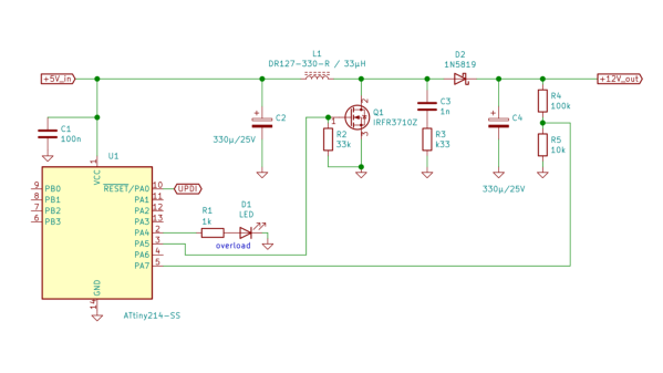
[SM6VFZ] designed, built and tested a switched-mode DC-DC boost regulator using the core independent peripherals (CIP) of an ATtiny214 micro-controller as a proof of concept, and it looks pretty promising!
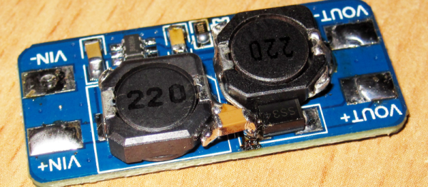
A Buck, Boost, or Buck-Boost switching regulator topology usually consists of a diode, a switching element (MOSFET) and an energy storage device (inductor/capacitor) in the power path, and a controller that can measure the output voltage, control the switching element and add safety features such as current limiting and temperature shutdown. A search for switching regulators or controllers throws up thousands of parts, and it’s possible to select one specifically well suited for any desired application. Even so, the ability to use the micro-controller itself as the regulator can have several use cases. Such an implementation allows for a software configurable switch-mode regulator and easy topology changes (boost, buck, fly back etc.).
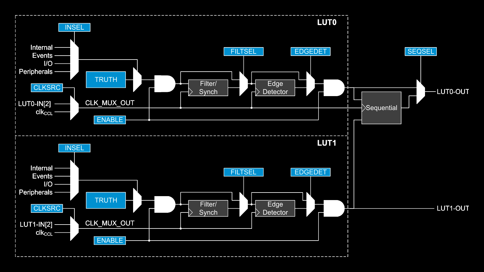
The “Getting Started with Core Independent Peripherals on AVR®” application note is a good place to get an overview of how the CIP functionality works. Configurable Custom Logic (CCL) is among one of the powerful CIP peripherals. Think of CCL as a rudimentary CPLD — a programmable logic peripheral, which can be connected to a wide range of internal and external inputs such as device pins, events, or other internal peripherals. The CCL can serve as “glue logic” between the device peripherals and external devices. The CCL peripheral offers two LookUp Tables (LUT). Each LUT consists of three inputs, a truth table, a synchronizer, a filter, and an edge detector. Each LUT can generate an output as a user programmable logic expression with three inputs and any device that have CCL peripherals will have a minimum of two LUTs available.
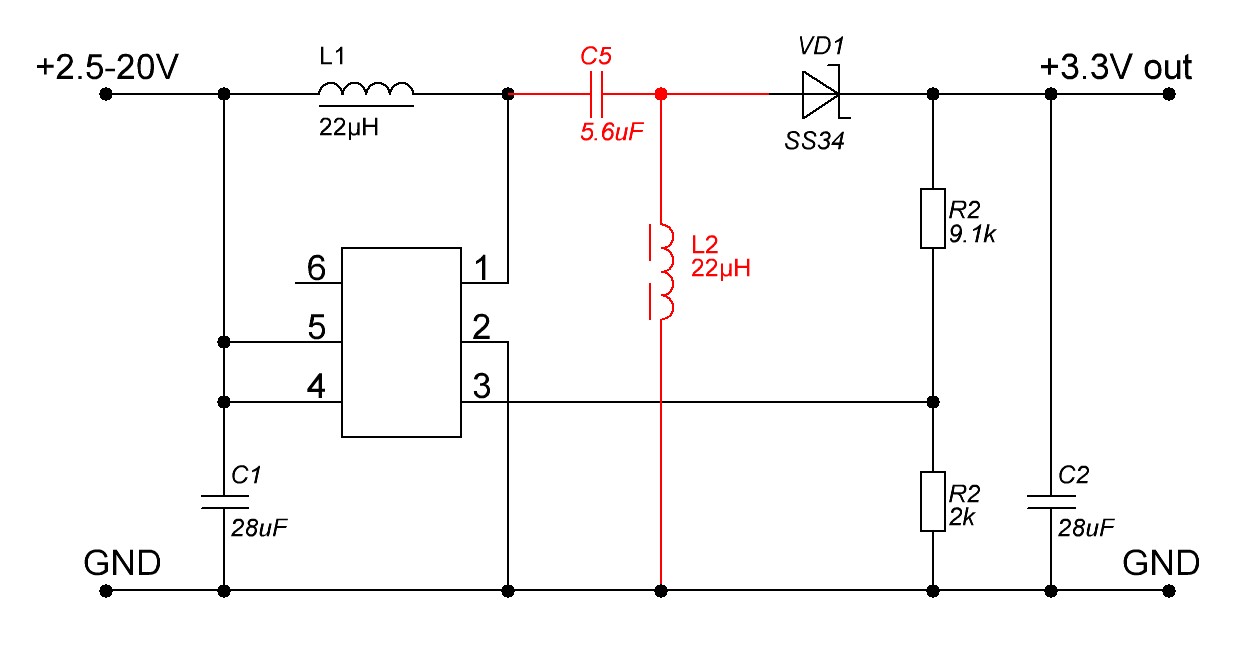
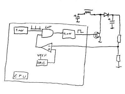 This napkinCAD sketch shows how [SM6VFZ] implemented the boost regulator in the ATtiny214. The AND gate is formed using one of the CCL LUT’s. The first “timer 1” on the left, connected to one input of the AND gate, is free running and set at 33 kHz. The analog comparator compares the boosted output voltage against an internally generated reference voltage derived from the DAC. The output of the comparator then “gates” timer 1 signal to trigger the second “timer 2” — which is a mono-shot timer set to max out at 15 us. This makes sure there is enough time left for the inductor to completely release its energy before the next cycle starts. You can check out the code that [SM6VFZ] used to built this prototype, and his generous amounts of commenting makes it easy to figure out how it works.
Based on this design, the prototype that he built delivers 12 V at about 200 mA with an 85% efficiency, which compares pretty well against regular switching regulators. Keep in mind that this is more of a proof-of-concept (that actually works), and there is a lot of scope for improvement in terms of noise, efficiency and other parameters, so everyone’s comments are welcome.
In an earlier blog post, we looked at how ATmegas with Programmable Logic came about with this feature that is usually found in PIC micro-controllers, thanks to Microchip’s acquisition of Atmel a few years back. But we haven’t seen any practical example of the CCL peripheral in an Atmel chip up until now.