Most of us make do with the VRAM that came with our graphics cards. We can just wait until the next one comes out and get a little more memory. After all, it’d be madness to try and delicately solder on new components of something so timing-sensitive as RAM chips, right?
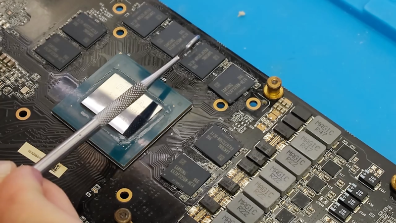
[VIK-on] took it upon himself to do just that. The inspiration came when a leaked diagram suggested that the RTX 2000 line could support 16 GB of RAM by using 2GB chips. NVIDIA never did release a 16GB version of the 2070, so this card is truly one of a kind. After some careful scouring of the internet, the GDDR6 chips were procured and carefully soldered on with a hot air gun. A few resistors had to be moved to accommodate the new RAM chips. During power-on, [VIK-on] saw all 16 GB enumerate and was able to run some stress tests. Unfortunately, the card wasn’t stable and started having black screen issues and wonky clocks. Whether it was a bad solder joint or firmware issues, it’s hard to say but he is pretty convinced it is a BIOS error. Switching the resistors back to the 8GB configuration yielded a stable system.
While a little more recent, this isn’t the only RAM upgrade we’ve covered in the last few months. Video after the break (it’s not in English but captions are available).
Thanks to Carson for sending this one in!


Now I’m thinking how great it would be if GPU cards came with some sort of standardized VRAM slots, to make upgrading them super easy.
You’re harkening back to the 80 and 90’s
Heh, I scraped at the solder on SOJ chips with an Xacto knife and pried the chips off a junker to get an extra megabyte into my VLB CL-5428 card, for 16 bit color at 1024×768 and double buffering at lesser res.
This immediately reminded me of the early ATI Rage cards that had something like a laptop RAM socket into which the video RAM was installed as a separate card.
Seen this too many time on reddit for people who don’t put in the engineering analysis.
You can’t put sockets:
– VRAM have very wide busses, so there are just too many connections to be made. i.e. long, high pitch, expensive
– Signal integrity issue at VRAM speeds – they are 5X speed of your regular DDR4.
– limited track length, sockets have stubs that can cause reflection – you know they had to drill off the via stubs on the 3000 series because of signal integrity issues. Think sockets would work!? – NO
– You don’t have space around the GPU – heat sink you know…
– VRAM changes. One minute, it is GDDR5, next it is GDDR6, GDDR6x.
The typical VRAM clocks are not much higher than GPU core clocks. Geforce RTX 2060 has max clock set to 1680MHz, and VRAM clock to 1750MHz. The problem is with memory width, which is typically 256 bits nowadays. The other problem is the heat dissipation. A good solution would be some CPU-style socket, like AM4 or LGA-1155. Routing and signal integrity would be an issue. Still it’s doable, but there is no money in it graphics cards manufacturers – they want you to buy the entire card, not just memory expansion module…
“The typical VRAM clocks are not much higher than GPU core clocks. Geforce RTX 2060 has max clock set to 1680MHz, and VRAM clock to 1750MHz.”
The bitrate on the memory for the RTX2060 is actually 12 Gb/s according to nVidia.
Reason for why it isn’t written as “12000 MHz” when dealing with various overclocking utilities is because there one isn’t effecting the bitrate, but rather the bus clock. And for DDR busses, the clock is half the bitrate. But on top of this, most GPUs have a fixed multiplier between the clock one sets and the actual memory clock, making the number far smaller yet again.
In short, your statement that “VRAM clock to 1750MHz” is on par with saying that the CPU runs at 100MHz, since the system base clock is 100MHz, neglecting any clock multipliers in the chain.
Also, unlike DDR4 that currently tops out at about 5.2 Gb/s, GDDR6 is a fair bit faster in comparison. (Except, 5.2 Gb/s DDR4 is practically “non existent” compared to the GDDR6 that is common as mud in comparison.)
In regards to bus width, 256 bits isn’t all that super wide to be fair. (Even the 3080’s 320 bit wide bus isn’t that gigantic either…)
Quad channel memory on CPUs isn’t uncommon, and each memory channel has 64 bits + their own addressing. Making it an even wider bus than what we typically see on VRAM. Not to mention how there is CPUs with more than 4 memory channels as well on the market. (Consumer platforms are though currently only having 2 memory channels. (Ie, AM4, LGA1151 and LGA1200.) And yes, DIMM slots should not be confused for memory channels.)
Downside with memory slots is though the following:
1. The least important thing. It impacts signal integrity. (One can use surface mount connectors to greatly reduce any stubs and improve signal integrity immensely, but it doesn’t take away all other parasitics of a connector. The use of SMD connectors is practically “required” for PCIe v4 and beyond. And has been pretty standard for motherboards supporting the higher RAM clock speeds.)
2. Connector cost. (Just soldering the chips directly onto the board is cheaper for some “odd magical reason”… To the degree were even some Server/thin-clients have soldered in RAM for the CPU, sometimes even a soldered in CPU. (Especially common in Laptops.))
3. Space. (Connectors and daughterboards takes up more room than having the chips directly on the board.)
It is mainly about reduced costs, and considering how both AMD and nVidia are both pushing their board partners to hit very tight price targets, then it simply isn’t room in the budget for upgradable VRAM.
(And for those running particularly memory intensive workloads, then one can to a large degree just shuffle data to and from main RAM if the application supports it, in other words going the GPGPU route. Making more VRAM partly unneeded, especially as PCIe v.4 is having far more bandwidth for such transactions.)
we can do it… The connectors will be very expensive, even so still probably can’t use GDDR6 as-is. Which means lowers performance (higher access times for different protocol that is more robust).
I think for very specialized equipment compromises on cost are reasonable, and even compromises on performance as long as goals are still met.
But if you’re making a consumer device to be fast and cheap(ish). You don’t really want to make those kinds of compromises.
Besides, it’s probably better to buy second (or third) card to add more memory. The driver is supposed to be able to schedule very parallel things like shader programs. And the newer cards can talk to each other over NvLink, not as fast as the local memory on a card, but it does make things like pipelined shaders, synchronization and semaphores practical.
I’d be fine with soldering…just make the BIOS editable…
I was only aware of some Matrox cards that did that.
I think the Matrox G-200 was the last of the all-new graphics cores launched to use it. While ATI Rage models had been having sockets and inline slots for a couple of years before and it’s last Rage models to support it were roughly contemporaneous with the G200. However it dated back at least to early SVGA card clones, which may have had DIP sockets to go to 512kB from 256 or 1024 from 512. I did however see a mention on .io of an EGA card that had expandable RAM.
I appreciate all the informed and informative replies from everyone. I did have similar thoughts, that it would be less efficient and more complicated engineering-wise, plus not make as much sense profit-wise for the manufacturers. Just wishful thinking I guess.
A slot would likely not work due to size and data rate constraints however they could certainly employ PGA VRAM modules and accompanying sockets while adding only about 1/8 inch of height (in many cases this would actually improve cooling as well due to a much smaller gap to fill in between the modules and the cooler with thermal pads .)
Could it be possible that there’s a hardware bug that prevents 16GB from working?
More likely the card firmware’s DRAM bus margining settings are tuned for the original 8Gbit part and the 16Gbit part is similar enough to work at all but different enough to be unreliable.
Somebody who speaks Russian should ask this dude if he’s using a ADATA SSD with old firmware.
It’s DRAM, so it could be an issue with refresh (ie, the refresh settings not being correct for 2x the memory).
Given it sorta worked, I would figure on there being a slight glitch with the timings, which might improve if you give it another 0.1V
I recall though on Radeon 8500 and 9500 series when ppl were trying to turn their 64MB cards into 128MB cards and hotair reflow was rocket surgery, that timings in the 128MB BIOSes were found to be looser, but there were BIOS editors that let you tweak.
I think that it is bad solder on BGA chips – he change resistors so it is raporting 16GB but if only one of data or adres lines is not or bad soldered then when test program try to write/read from for example upper regions of memory it crash.
Is HaD suggesting I do this because I don’t have enough black screens?
I bet signal integrity incompatibility issues between the different memory chips are at least contributing to the instability if not the direct reason. I’ve only done DDR4 designs but the amount of trace tuning required to achieve our targeted margins on those lines is pretty in depth and probably account for the majority of simulaiton work we perform on our digital boards. I’ve seen issues arise where SI takes a hit just between different revisions of the same chip, let alone an entirely different brand/size. Our tuning requires die-to-board and routing models and we very rarely target mutliple chips as it’s very difficult to incorporate multiple near-contradicting requirements (although we’re probably targeting more robust margins than commercial) and DDR6 is way faster than DDR4.
This is not an upgrade.
The thing not working (properly) with 16GB is likely the reason that Nvidia never sold them.
This is destruction of a (presumably) working videocard.
Why is it not labeled as fail of the month?
I did a quick look , and video cards with >8GB memory start at around EUR800.
Buying RAM from AliExpress, expecting it be flawless….. That’s the problem.
Fail of the month? Seriously?
No magic smoke and he reverted back to fully functional state by simply resoldering jumpers back to 8GB configuration. If he finds a better firmware or figures out it needs a bit more juice it’s back to 16GB by simple jumper resoldering. Also, some mad soldering skills there, working with BGA more comfortably than most people are with TH.
i like jobs like that, im wondering if the hacker scene could address the soldered ram on laptops nowadays. if we have more open diagrams, upgrading soldered ram will be just a sake of a steady hand and a hot air gun.
I know Greg Davill is doing that right now with his XPS
At least they didn’t have to use the micron ram :(
It is good video
Hi . Can you post link where to buy memory to grafic card or seller site?
I do these mods daily and tinker all day. He is correct, until we get software guys at Nvidia to release the BIOS for modification we can solder stuff like this all day, but can we qrite the firmware to support is the real question. Solderijg and replacing chips is dirt easy…
Interesting. I have two broken 780’s here which could well benefit from more vRAM as the existing chips are old and clapped out.
In this case, the hack would be increasing the capacity AND hacking the vBIOS to support the extra memory.
6GB 780Ti anyone? Bwahahahahaha.