In 2018, when KiCad Version 5 modernized the venerable 4.X series, it helped push KiCad to become the stable and productive member of the open source EDA landscape that we know today. It has supported users through board designs both simple and complex, and like a tool whose handle is worn into a perfect grip, it has become familiar and comfortable. For those KiCad users that don’t live on the bleeding edge with nightly builds it may not be obvious that the time of version 6 is nearly upon us, but as we start 2021 it rapidly approaches. Earlier this month [Peter Dalmaris] published a preview of the changes coming version 6 and we have to admit, this is shaping up to be a very substantial release.
Don’t be mistaken, this blog post may be a preview of new KiCad features but the post itself is extensive in its coverage. We haven’t spent time playing with this release yet so we can’t vouch for completeness, but with a printed length of nearly 100 pages it’s hard to imagine [Peter] left anything out! We skimmed through the post to extract a few choice morsels for reproduction here, but obviously take a look at the source if you’re as excited as we are.
There’s No Place Like (0, 0)
Starting with the foundation, KiCad 6 will finally bring a configurable coordinate system! We’ve found that a significant stumbling block for new users is that the default KiCad coordinates start at the upper left instead of the lower left, as in most CAD and drawing tools.
Version 6 will allow the user to relocate the origin as well as flip either axis, allowing for maximum ordinal freedom. Clearly it doesn’t take much to get us excited, does it?
Rounding Traces and Filling Zones, Mostly
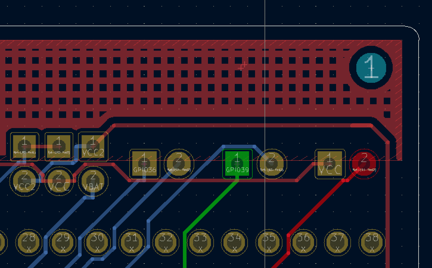
Another historically missing feature in KiCad is curved traces. V6 moves part of the way there, allowing traces to have rounded fillets. This doesn’t quite get to the groovy curvy traces of the 70s but it’s progress in the right direction.
Along similar lines there is new variety in the way a zone can be filled. Now instead of being forced into a solid fill there is a second choice; hatched fill! We say the more the merrier! Next stop; hearts, stars and horseshoes?
Getting Together with Groups
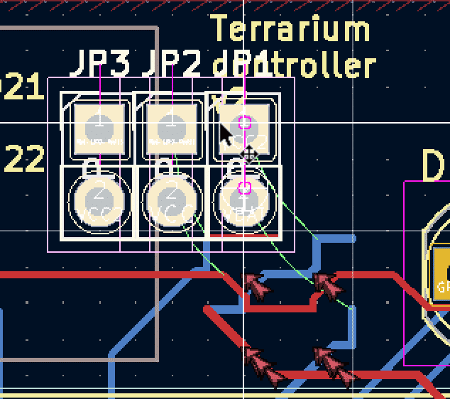
It may seem minor, but should be appreciated by anyone who has worked with carefully arranged groups of components during layout; items can be grouped! It’s always been possible to select multiple elements and drag them together, but that grouping was lost as soon as the selection changed. In KiCad 6 components can be explicitly grouped, allowing you to move those pesky headers around all at once, in perpetuity.
Bussing in the Signals
Even after using version 5 for years, signal busses in KiCad schematics seemed like an ugly duckling with a usage so awkward that they weren’t worth using. [Peter]’s overview has taught us a few new things about that older tool that we didn’t know under the rubric “enhanced bus handling”. For instance, the older version 5 allows the user to textually specify net names to connect across a bus instead of forcing the use of bus entry connections and individual net labels.
Version 6 makes busses significantly more powerful. It’s now possible to specify more elaborate and less uniform net names that share a single bus, and there are graphical hooks in context menus that allow you to “unfold” individual nets from the bus without the guesswork required in version 5. And as an added bonus, in version 6 the visual style of busses can be changed. We’re excited to start getting our signals together!
That’s Not All Folks
Whew, what a list! And that was but a tiny fraction of the improvements in KiCad 6, or the coverage from [Peter]’s excellent post.
It’s worth noting that the post is based on nightly builds euphemistically versioned 5.99. Until the release is officially cut, features and functionality are subject to change, but everything is publicly available to try out in the nightly builds if something catches your eye.


Does it have a unified interface and shortcuts across eeschema, pcbnew and the library editors?
Oh, looks like they’re dropping the mouse-over keyboard actions that I liked. That means a lot more clicks will be required. Bad! Soo Bad! Not good!
That’s an already reported bug
If they do this Kicad will suck. Dude, Kicad was the best CAD just because of that. Some features must to remain because they improve the usability. And now what? Maybe they are going to move to a binary file format too. I hope they keep the good old features, because they make Kicad the best.
Without text-based format option, I would’ve been unable to do the PCB motor I designed. Used Python to manipulate the text in a KiCAD file to make arbitrary trace paths and shapes defined parametrically (like 2D CAD). Binary would be INSANELY harder to reverse engineer like that, and KiCAD still has a very poor interface for making arbitrary trace layers.
which do you mean? I gave the nightly build a try and could do things like move/rotate the component my mouse was over when I didn’t have another component selected
Yeah mouse over key actions is the key to speed and efficiency. I found that needing to click on the object in PCB new on the latest v5 has been killing me.
i feel like once there is official support for a user-maintained component database, similar to altium DBLib, I’m going to wait to make the jump.
I’m not sure I follow, as KiCAD and it’s component database are already user-maintained. I assume you mean something else though.
I think he is talking about an online database that is shared. So when you add a new component, I also have it (for example).
so do a pull request and it’s merged into the database.
Otherwise you will end up with 42 same crap component.
tru dat. after dealing with crap library components in Eagle for years, I think it good that Kicad has a process that has a high bar.
I’m hoping that support for multiple versions gets better. That is particularly important for commercial use.
With old software it’s common to keep old versions of the IDE and compiler around so it can be maintained without having to update it to the latest, which can introduce bugs or cause problems getting it to build. On the embedded site many IDEs support multiple versions of the supplied include files as well, so you can build with the same library versions and header files you tested with a few years ago.
In Kicad you end up having to upgrade your old projects and resolve parts that have changed, as well as hoping that the upgrade process is flawless.
I jumped ship back to Altium, because of the limitations that Kicad 5 still had. It has taken way too long for the coordinate system to be put where it is supposed to be.
Finally the rounded traces have made the appearance, as well as the hatched copper.
It would be nice if teardrops became part of the tool as well.
The library structure is still one large flaw of Kicad, and makes it very difficult to work across different machines/users. The other thing that I believe is still missing is support for flex-rigid stacks.
But
for the price you pay, it is a pretty fine tool.
I always copy footprints to a per-project library and just consider it to be part of the project. Otherwise a footprint gets deprecated, KiCad gets updated and the PCB needs redesigned. Maybe the replacement IS better but I don’t want to be forced to update all my old designs just because I dared update KiCad. It’s bad enough when my Linux distro’s package maintainers do that!
I wish there was a one-click way to do this. I’ve been setting one of each footprint in CvPcb then opening each in the footprint editor, saving it to the local library then re-setting all the footprints to the new local copies in CvPcb. I wish there was just a single button in CvPcb that would copy the selected footprint to the local library and then set it to the copy. Bonus points if it would recognize when there already is a copy in the local library and just automatically use that.
Or maybe there is a better way and I just need to learn it? I’m still kind of new at this.
I cannot agree more!
Kicad V5 is already pretty usable, has some flaws such the mouse warp, single font, no grouping, etc…
But the components & footprints management is terrible, no way I’m using the online version as it can get overwritten overnight and need a board redesign.
The only solution is local copy, shared over project & users but it’s a PITA to maintain, I really wish it was easier as suggested.
Interesting perspective. Having previously been an Altium user and fan, KiCad has totally won me over. I actually prefer the KiCad library organization. Not to mention it runs way faster and is far more stable than Altium, which tends to crash at least once a day in my experience.
Just stopped by to say I love KiCAD.
We’ve used git to handle shared kicad symbol & footprint libraries. Seems to work so far. Even using git to switch between board designs when I need to work on a different board.
Hackaday article describing it but not an Intro to it –
https://hackaday.com/2018/09/19/advanced-techniques-for-using-git-with-kicad/
Useful –
https://jnavila.github.io/plotkicadsch/
@elmesito: Teardrops have been part of KiCAD for a while, thanks to [maui]. KiCAD should be thought of as an ecosystem. Because KiCAD is open source, third parties can easily write plugins for it, so is not only the “core” KiCAD that should be considered, but also the plugins. Teardrops, via stitching, RF tools, parts assistant, even an autorouter have all been there for a while. Here a useful URL about KiCAD plugins, including teardrops. Some things may change due to the upcoming 6.0:
https://hackaday.com/2019/11/19/kicad-action-plugins/
Until they implement the componet style library for new parts like eagle or altium I’m gonna pass it.
Good update nevertheless
It is open source, so they are three ways for what you wish was added to happen. Wait until someone else decides to implement exactly what you want in the exact way that you want. Wait until someone else decides to implement something similar to what you want that functions in the some way similar to what you want. Join the team and help and help them.
Or pay them/financially support the core developers. Usually this option is the best for the software and the community.
Touting “truths” like these is why The Year of Linux never happened.
^ This. I wonder in how many projects does “Truth” contribute code on.
Or just spend some money and have usable software and move on with life. I wonder where people find all the time to work for free on open source projects. Priorities I guess.
If you can afford Altium then you are coming from a very different perspective than most of us mere hobbyists.
CircuitStudio from Altium. 500 dollars
I actually have a perpetual Altium license in my company. But I use eagle in my personal projects. But the only reason I use Eagle and not kicad is because or the library system. Eagle is so simple and awesome.
I’m with you, Luis. I love EAGLE, and I am lucky enough to have a license to EAGLE 7.1 or so. This means, it’s nagging me that upgrades are available every time I start it, but it also means, I can just click “OK” and keep using it…forever. No subscription models for me, thanks!
Altium was ok, but there are still some things I never figured out about it. I’ve never tried Kicad, and won’t have a reason to for a long time. I suppose someday I’ll find something I just can’t do in EAGLE and can’t find a .ULP for, but it hasn’t happened yet.
I use Macs, the clock is ticking on how long my copy of Eagle 7 will be runnable as an x86 build. I used Eagle for 20 years, but I’m slowly migrating to software that I can download and build. Now that’s forever.
“Eagle is so simple and awesome.” — And there are some of us who have NEVER felt that way.
Disagree. I was very skeptical of KiCad’s library system but having used it I now actually prefer it.
Can’t love it, I think it is the worst library system ever made
Since Kicad 4 and probably earlier you can have a component style library it just doesn’t force you to do it. You can have p/n, symbol, footprint, step file, documentation, pricing, or whatever custom field you want all linked to a specific schematic symbols that carries through everything.
But that’s the thing. It shoudn’t be linked to the symbols. It should be a top level component that have one or more symbols, one or more footprints and all the p/n, price etc associated to it.
This is the way.
They even have an official solution about it ( https://kicad.org/libraries/klc/S2.3/ ), and yet don’t seem to admit that this is a gross hack instead of an actual solution. I shouldn’t have to think about the footprint at the schematic stage, and it definitely shouldn’t be easy for me to accidentally pick the wrong one.
Almost throwed up seeing that. So horrible
So what’s the advantage of hatched fill anyway?
Ok. I LMGTFY’d myself and there seems to be quite a lot written on it.
For those who don’t want to look it up, I could gather that you would use it for:
– touch sensors (increased capacitance?)
– controlled impedance (black RF magic)
– flex PCBs (less chance of cracking)
– reduced thermal mass
Please note that you should not use it if you don’t know why. Signal integrity decreases, crosstalk increases, EMI increases. From a practical perspective, it has a very niche use.
Similarly, don’t split ground planes, try to keep all signals above a ground plane and far away from each other, route power traces rather than adding a power plane. There are various videos explaining why (see Altium).
WIshlist based on how Cadence Allegro works: grouping where I can choose to rotate the whole group, or grouping where I can choose to rotate each element selected around its midpoint. SImilarly, filtered grouping, where I can choose ‘only select text’ and then select the whole board and change the font size so that every refdes is the same, or rotate all the refdes in one section around their midpoints and drag them all up slightly. On big layouts, filtered select is so nice: I love being able to delete all traces in an area without deleting parts as well, or offset a whole portion of refdes from a packed-as-tight-as-PnP-can-manage into a non-critical area that has room and have them maintain alignment.
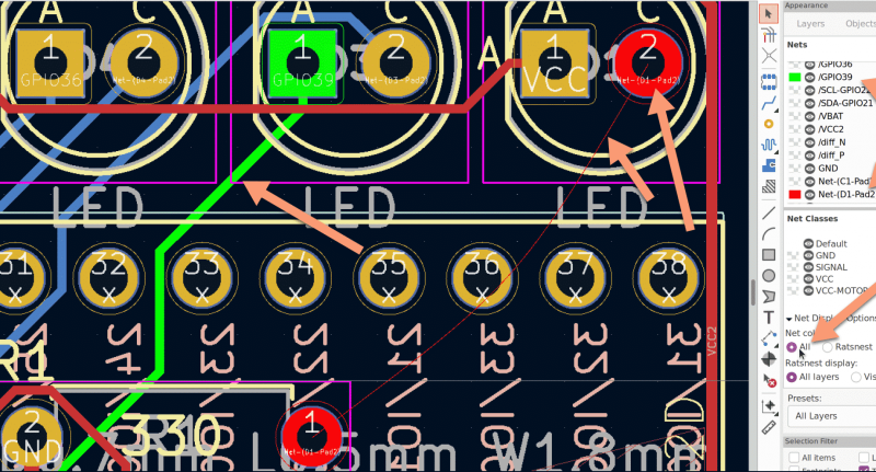
oh yay! you can toggle visibility of individual nets on the right panel! I got bogged down while trying to lay out a board with a couple hundred components because the ratsnest for GND net was too much noise. I ended up writing a little shell script to remove the GND net entirely from the file and then add it back after I got most of the other nets untangled. having this UI makes it so much easier to just focus on laying out the parts of a board I want to think about at any given moment.
fillet improvements are nice but not quite the same as the nicer curved traces from https://mitxela.com/projects/melting_kicad
looking forward to eventual support for splines in the editor so we don’t have to approximate curves with small lines
I’m most interested in UI improvements. If the UI isn’t as good as LibrePCB, I’m sticking with that. Maybe I’d learn KiCad if I was doing some insane 8 layer stuff that needed all those features, otherwise, I don’t particularly care to put in the weeks and weeks of learning time to figure out Vim4PCBs
It would be nice to see enhanced graphical and font imports. The current workflow for such things is very clunky, and getting desired results first time round is unusual. Direct scalable PDF imaging would enable vintage circuit replication, and give the pcb arts communities a big leg up.
For all those that are missing a proper component library management, take look at https://horizon-eda.org/
wow thanks for sharing. It looks awesome
> Now instead of being forced into a solid fill there is a second choice; hatched fill! We say the more the merrier! Next stop; hearts, stars and horseshoes?
Design aside is there any upside to use hatchet fill instead of solid fill? Any manufacturing/electrical advantages?
I looks nice I guess, other than that I’m just as confused about that one myself.
I’ve seen mentions of things like dealing with unbalanced thermal expansion/contraction on larger boards.
The main reason is copper balancing – thermal warpage, etching etc.
It also helps as a solid fill plane (vs a hatched fill) would be too stiff on a flex PCB. I do hope that they would allow for being able to rotate the hatches as well as the geometry.
Yes, flex PCB. Rigid PCB, pretty much just showing off.
You can keep most of your RF isolation, but not have to deal with the additional thermal mass. This means the solder profile will be easier since the infill will heat up easier/faster.
Hatched ground plane can reduce trace capacitance while still providing that shielding goodness. You’ll often see it specified in reference designs for capacitive touch circuits.
The other features are nice truly, but dear God…
Autorouter with out wacky hacks!!! Please
Personally I have no use for a full board autorouter, but it would be handy for certain areas or hand picked nets. After all, you should not mix analog, low speed digital and high speed digital signals, grounds need to be done properly and so on.
I get that autorouters can be messy.
But that’s why a automatic and manual hybrid approach should be used in conjunction.
Because in the end they improve the presentation of the board and cut down on unnecessary vias.
Which is the most leads to the most important reason, saving money on having the board fabricated.
Yeah. I’ve wondered about this as well. How useful is a full board autorouter?
Any time I’ve tried on a board with less than 4 layers, it ends up very messy, to the point where I wouldn’t actually use it (power daisy-chaned on thin traces with no regard for currents, etc.)
I do like the interactive routing once I got used to its quirks, and after some further improvements, I wonder if it could have an interactive auto-route added, where you could just click the endpoints and it would auto-route that specific trace.
IMO, the interactive routing is really where it’s at, and I think some improvements to that would be much more beneficial, though I would like to see that improved a bit. Currently if routing long traces, you have to click fairly frequently to keep it from getting stuck, then jamming up for a second, and coming up with a really dumb solution. In a lot of cases it’s mostly just about running a trace between a whole bunch of other ones where you never left space, so the shoving could probably use some sort of locality preference where it doesn’t focus as much on things further back near the start of the track, and prioritizes making room where you’re currently trying to run it.
There never going to implement a native autorouter dispite the fact it’s probably the most requested feature and probably the biggest thing keeping it out of the big leages.
They need to listen to the community more about that, and stop being pig headed about it.
Actually, nobody has requested that feature on the issue tracker as far as I can tell. There are many other highly-requested features that are being used to plan development work for future versions, though, so it seems like other people may have different opinions about what is keeping KiCad from the “big leagues”…
https://gitlab.com/kicad/code/kicad/-/issues?label_name%5B%5D=feature-request&scope=all&sort=popularity&state=opened
You should take a look at how many people are installing the plugin to get around that.
No discussion I have even be involved with had people happy that they have to jump threw extra hoops about it. Some maybe settle with the plugin, and most probably don’t submit a feature report. But the community feeling about it seems pretty darn clear to me.
Separate autorouters still exist for the “big leagues” market because sometimes the bundled autorouter just isn’t enough for the job. We use that for our designs – so big that they have to compile a larger version of the standard PCB package for us.
Autorouter gripes aside. I should be clear in saying I really like kicad.. Love how everything connects together using a project workflow where one thing updates the other.
Nope. You still need to export, import into freeRouting, route, export, import to KiCad. Annoying
As a consultant that occasionally designs a PCB, KiCad is perfect. I love saving thousands of dollars over Altium and the other outrageously priced tools.
I’ve been using KiCad quite a bit for a few years now, and overall it’s getting pretty good. A few of the new features, like being able to hide specific nets (get the GND ratlines out of the way while you route the rest of the board), and better selection filtering will be a big help.
I’m curious if there’s been any improvements to the trace neck-down behaviour, or lack thereof. There’s lots of times that traces need to be larger than the pads they connect to, and in kicad 5 there doesn’t seem to be any way to do this automatically, which also makes the net classes a lot less useful.
Typically for those I’ll end up drawing the trace first, then deleting the ends, then resizing it to the proper width and clearance. and then reconnecting the ends with thinner traces again. it’s always kind of fiddly, and can be a real mess at times.
It would be awesome if there was actually a tapered neck-down segment or something along those lines, so you could have a reasonably smooth connection between a thin pin on a qfp to a large power or impedance controlled trace. Even with the current hacks I use the results are a bit ugly, usually a thin trace going into a big round end of the larger trace.
I had a link to a router that could layout similar to the old school ‘tape’ laid boards (ie: traces that were more splines rather than arcs), but lost it when windows did an autoupdate and subsequently trashed (ie: erased without backup) all my open pages. I was looking at purchase until then!
I think it was stand-alone, and it could do push/shove and would export results so they could be used in packages like altium & kicad.
Anybody got any clues? I’ve searched and searched but can’t find it.
Finally found it!
“TopoR”
Thank you to all the developers that made this happen! I have been running the nightlies and they are such a joy to use.
I really hope that someday there is a rock solid way to generate fabrication outputs, renders and difs using the python bindings so that I can get Gitlab to run some continuous integration scripts on each push. You can then link to those images and files in the readme of your project and it keeps things nice and up to date. There are some hacky ways to do that now but they break too often.
Here’s an example I made: https://gitlab.com/damped/denfordcnc
You can see the scripts that make it work in .gitlab-ci.yml
Man, it’s kind-of hidden most of the way down in the “other improvements” section, but the streamlining of copy-paste between projects for PCBNew and, more importantly, EESchema is a game-changer for me. Working from smaller dev boards to larger projects often has me replicating work in V5. Maybe I should move to 5.99, I’m about to do the same once again.
I moved to Kicad from Eagle in about 2013. It was hard at first, but I found it to be worth the effort. And since then, Kicad has just got better and better, while it sounds like Eagle has (since the Autocad buyout) become progressively more hostile to hobbyists and casual users.
A huge thank you from me to the generous people who work on continuously improving Kicad! I am excited about the upcoming version 6!