
We’re accustomed to seeing giant LED-powered screens in sports venues and outdoor displays. What would it take to bring this same technology into your living room? Very, very tiny LEDs. MicroLEDs.
MicroLED screens have been rumored to be around the corner for almost a decade now, which means that the time is almost right for them to actually become a reality. And certainly display technology has come a long way from the early cathode-ray tube (CRT) technology that powered the television and the home computer revolution. In the late 1990s, liquid-crystal display (LCD) technology became a feasible replacement for CRTs, offering a thin, distortion-free image with pixel-perfect image reproduction. LCDs also allowed for displays to be put in many new places, in addition to finally having that wall-mounted television.
Since that time, LCD’s flaws have become a sticking point compared to CRTs. The nice features of CRTs such as very fast response time, deep blacks and zero color shift, no matter the angle, have led to a wide variety of LCD technologies to recapture some of those features. Plasma displays seemed promising for big screens for a while, but organic light-emitting diodes (OLEDs) have taken over and still-in-development technologies like SED and FED off the table.
While OLED is very good in terms of image quality, its flaws including burn-in and uneven wear of the different organic dyes responsible for the colors. MicroLEDs hope to capitalize on OLED’s weaknesses by bringing brighter screens with no burn-in using inorganic LED technology, just very, very small.
So what does it take to scale a standard semiconductor LED down to the size of a pixel, and when can one expect to buy MicroLED displays? Let’s take a look.
All About the Photons
The most important property of a display is of course the ability to generate a sufficient number of photons to create a clear image. In the case of CRTs, this is done by accelerating electrons and smashing them into a phosphor layer. Each impact results in a change in the energy state of the phosphor molecule, which ultimately leads to the added energy being emitted again in the form of a photon. Depending on the phosphor used, the photon’s wavelength will differ, and presto, one has a display.
The reason why CRTs are rather bulky is because they use one electron gun per color. While this is fairly efficient, and the use of electromagnetic controls make for impressively fast scan rates, it does give CRTs a certain depth that is a function of display dimension. An interesting improvement on these classical CRTs came from Canon and Sony in the form of SED and FED, respectively during the early 2000s. These display technologies used semiconductor technology to create a single electron gun per pixel, which would fire at the phosphor layer, mere millimeters away.
By that time LCD technology was already beginning to become firmly established, however. Unlike like the somewhat similar plasma display technology, SED and FED never made it into mass production. Even then, LCD technology itself was going through some big growing spurts, trying to outgrow its early days of passive matrix LCDs with slow response times, massive ghosting and very narrow viewing angles using primitive twisted nematics (TN) panels.
Even though LCDs were clearly inferior to CRTs during the 1990s and into the early 2000s, what LCDs did have, however, was thinness. Thin enough to be put into mobile devices, like laptops and the ‘smart assistants’ of the time, such as personal digital assistants (PDAs). As LCDs gained features like active matrix technology which removed most ghosting, and new liquid crystal alignments (e.g. IPS, MVA) that improved viewing angles, so too did their popularity grow. Clearly, bulky displays were to be a thing of the past.
The Curse of the Backlight
An LCD has a number of layers that make it work. There is the liquid crystal layer that can block or let light through, there are also the color filters that give pixels their colors, and the TFT control and polarization layers. Most LCDs use a backlight source that provides the photons that ultimately reach our eyes. Because of all these layers in between the backlight and our Mark I eye balls, quite a lot of energy never makes it out of the display stack.
In the case of a ‘black’ pixel, the intention is to block 100% of the backlight’s energy in that section using the LC layer. This is both wasteful, and since the crystals in the LC layer do not fully block the light, LCDs are incapable of producing pure blacks. While some LCD technologies (e.g. MVA) provide a much better result here, this comes at compromises elsewhere, such as reduced response time.
This illustrates the most fundamental difference between a CRT display and an LC display: a CRT is fundamentally dark where the electrons don’t hit. SEDs, FEDs and plasma displays are also self-illuminating, as is OLED. This is a crucial factor when it comes to high dynamic range content.
With the move to LED-based backlights for LCDs, the situation has improved somewhat because an LCD can have different backlight sections that can activate separately. By using more, smaller LEDs in the backlight the number of so-called dimming zones can be increased, making darker blacks. You can see where this is going, right?
The Future is Self-Illuminating
After decades of display technology evolution, the factors which determine a display technology’s popularity essentially come down to four factors:
- How cheaply it can be produced.
- How well it reproduces colors.
- How well does it scale.
- How many use cases does it cover.
In the case of LCDs over CRTs it was clear why the latter couldn’t compete, and why plasma screens never made a big splash. It also makes it clear that – as demonstrated by e.g. Samsung exiting the LCD market – LCDs have hit somewhat of a dead end.
MicroLEDs were invented over twenty years ago, and while e.g. Samsung’s The Wall is seeing limited commercial use, the most exciting development will probably come this year, with MicroLED TVs that fall into the ‘affordable’ range appearing, assuming one’s target is a 76″ MicroLED TV for roughly what an early plasma display would have cost.
Smaller MicroLED displays are unlikely to appear for a while. Immature manufacturing technologies and the need to reduce pixel pitch even more are the bottlenecks at the moment. This latter point is quickly seen in the specifications for Samsung’s MicroLED TVs to be released this year: they only support 4K, even in the 110″ version. At 50″, 1080p (‘fullHD’) would be about the most one could hope for without sending production costs skyrocketing.
A Matter of Time
As cool as new technologies can be, one cannot expect them to fall off the production line one day, all perfect and ready to be used. Early CRTs and passive matrix LCDs were terrible in their own unique way . As the technology matured, however, CRTs became reliable workhorses at very affordable prices, and LCDs became pretty tolerable.
OLED technology started off with an optimistic ~1,000 hour lifespan on the early Sony prototypes, but today we see (AM)OLED displays everywhere, from cellphones to TVs and even as tiny monochrome or multi-color screens for embedded applications. With MicroLED having the benefit of being based on well-known semiconductor technologies, there’s little reason to doubt that it’ll undergo a similar evolution.
As MicroLED features higher brightness and longer lifespan that OLED, with lower latency, higher contrast ratio, greater color saturation, and a simplified display stack compared to LCDs, it’s little wonder that MicroLED displays are being produced by not only Samsung, but also by Sony (‘Crystal LED’) and AU Optronics, amidst a smattering of other display manufacturers, and tantalizing promises of small (<5″) MicroLED displays.
We know that everyone likes lots of tiny LEDs. Will your love last, once they become this commonplace?


That does sound promising, and is an idea that I had never considered. If the microLEDs are anywhere near as robust as the epoxy coated ones we’re all used to seeing, these displays could last darn near forever (but the power supply will go up in smoke from a dead capacitor 15 minutes after the warranty expires).
They’d last so long that TV manufacturers will probably conspire to bury this very deep. Has happened before.
LCD screens with LED backlights can last a long time too. And honestly, modern LCD screens are already more than fine for me.
But we needn’t worry about manufacturers creating an eternal TV and going out of business. How often are TVs actually fixed these days? Cheap capacitors only last a few years. They aren’t hard to replace but how many units how junked because “it’s not worth it”? Custom ICs can also have short production lifetimes making controller board repair unlikely. And companies can make your TVs “smart” and reliant on webservices that eventually disappear. Samsung has darn near perfected the art of making good products that require replacement not because their new products are so awesome but because they simply turn off support on the old ones.
solid polymer capacitors are becoming the norm in high stress applications such as computer motherboards, and supplanting the electrolytic. now if only they were used in internal power supplies for the same reasons….
Many manufacturers don’t make their money on the TV itself these days anyway. A failing TV would interrupt the tracking of your viewing habits that is their real source of income. I don’t think we have to worry about them burying more-dependable versions of a loss-leading product.
They don’t need to. They have already found a way to limit the lifetime of TVs. “SmartTVs” after 3-5 years no software updates, sluggish and dated UIs will make people upgrade long before the end of life of the actual display. On the other hand dumb TVs you can use till they just flat out die, plug in a Chromecast / Roku / Firestick for the smarts and just chuck that part in the trash when/if the manufacturer stops updating. I still have the 1st LCD TV i bought around the mid 2000’s one of the 1st 32″ TVs to support 1080p, a Sharp Aquos that still works to this day. It is now my bedroom TV. Went with a projector in the living room not to deal with the smart tv crap that’s out there these days and to have a bigger screen for the money.
Problem is the quantity of leds. FullHD is 2M pixels, 4(rgbw) leds per pixel.. So at least 8 milion leds in single display. Even with 10M hours MTBF leds you would get thousands dead subpixels per year.
They will need to reach trillion year MTBF led subpixel to reach current LCD state: No dead (sub)pixels for entire lcd lifetime in most sold units.. (until the capacitors stops capacitating..)
I assume they are totally aware of a proper failure rate and they have to catch up what consumers are used to nowadays. Think of what we accepted 15Years ago :D “less than 5 dead pixels… wow”
But why w? I think they will mix rgb, creating a w in micro-leds would add to much size and complexity to get the luminescent part into the space.
But event this 3/4 factor will not drop the MTBF significantly enough though.
Not entirely accurate. in the world of direct view LED displays (big honking video walls) we see walls with resolutions in the 10k range and beyond. and you might see a dead pixel or two/year appear. so the quality/QA is already there or almost there. only thing we are missing is the scale needed for consumer manufacturing.
Also in the direct view market, we only use RGB LED’s. not the RGBW arrangement.
i work for a company that manufactures direct view LED product.
I think they’ll need to go the RGBW. Most other commercial HDR product are now RGBW, even higher end LED strips are mostly RGBW, and brightness of most expensive TV can’t be lower than current LG RGBW OLEDs. And as bonus, it will reduce the driving current of RGB leds which in turn will increase the MTBF.
LED failure rate increases with higher temperature and with currents closer to maximum allowed brigtness. 4K TV screens are usually between 2 and 4 pixels per mm. With this density, I don’t think you can provide comparable cooling to the LED billboards. (but they make my eyes bleed, so maybe you can). All the big led panels I saw, were not made for image and color quality, just for pure annoing brightness, and usually I can see R, G and B points bleeding through other colors.
I am not worried about the driver transistors, because this is alredy solved in current LCDs and OLEDs, every subpixel already have at least one.
Driving current per LED must be small anyway. If you think a 1080p screen with ~6M LEDs with only 1mA/LED would be 6000A at max, or around 18kW at full white. That would be really blinding in a living room and turn it very quickly into a sauna. I think we have to reduce this by about two orders of magnitude to 10 or 20µA per LED.
Most LED strips with RGBW do it to conserve energy, why burn 3 leds to make white when you can use a 3rd of the power burning a single white LED. It also prevents the rainbowy offset shadows that can come from non diffused RGB LEDs being lit simultaneously to create white. RGBW is likely used in OLED displays so that the RGB subpixels don’t have to be driven as hard to create white thus improving the degradation rate of the OLEDs. Plus it keeps your whites from color shifting as the subpixels degrade. Not sure if it is still the case, but the blue OLED subpixels were usually the ones to degrade the quickest, so that means an all white screen would start shifting over into the yellowish spectrum as the blue subpixels degraded. a white OLED subpixel would just decrease in brightness as it degraded, rather than color shifting. Another trick they could be doing with the RGBW OLEDs is having a lower “color resolution” perhaps the panel is a true 1080/4k worth in white OLED subpixels with half the number of color subpixels, lowering the subpixel count that needs to be driven. This is somewhat like how the old analog NTSC worked, where the B/W signal was at full resolution/bandwidth and the color bandwidth/resolution was somewhat less. Humans perceive sharpness more from a monochrome signal. Then you can pepper in the color at a lower resolution and it still looks fine.
That’s assuming the MTBF counts totally random failures instead of a wear-out mechanism.
In other words, what’s your failure distribution around the mean?
And the failure model. Pixel stuck permanently to red on LCD annoys much more than dead OLED pixel which is just a non-illuminating black dot.
I’m estimating LED failures (black subpixels). Bright subpixels are caused by malfunctioning transistor and “printed” transistors are already (mostly) solved in current LCDs and OLEDs.
I didn’t think about exact failure distributions, impact on whole product or anything similar, I was just ilustrating, that microleds probably have to be more “robust than the epoxy coated ones we’re all used to seeing” and they will no be anything close to “these displays could last darn near forever” even when considering LEDs alone.
Samsung “The Wall” microLED TVs seem to manage just fine.
RGBW is nice for illumination, but for a display RGB is enough since decades.
This really would be no different than OLED displays’ OLED displays are already a single LED per pixel, they are just of the organic variety rather than in-organic variety. If this were an issue you’d see OLED screen phones with hundreds of dead pixels all over them after a year or so of use. Yes OLEDs degrade with use, but I’ve not seen OLED phones with just plain old dead pixels peppered all over the screen
One thing I notice is that the first digit of green LED 7 segment display on my 20 years old microwave is much brighter than the rest. The intensity degrades over usage even for ones that doesn’t get pushed to its limits.
Why exactly the first?
Are you sure this is green LED and not a vacuum fluorescent display? The VFDs ahve much stronger wear out effect.
I would guess it is VFD as well. VFDs degrade with usage much the same way OLEDs do, since the phosphor in them is organic as well. LEDs in indicators/7 seg displays are driven at such a low power they’ll pretty much last forever and not degrade. LEDs pretty much lasted indefinitely until we started coming out with higher brightness ones for area lighting and we are now pumping watts though the LEDs rather than a few miliwatt for an indicator LED. All the extra power and improper cooling is what kills today’s high brightness LEDs. Many VFD dotmatrix display panels have functionality to invert the image every so many minutes to wear level the pixels, though most people don’t use it. Depending on the content being displayed this inverting may or may not be an issue. If you’re just mainly displaying text then you’re just cycling between light txt on a dark background to dark text on a light background.
Due to component size, at this point it’s just be large scale microfabrication and it’s a testament to machine precision. However, I’m assuming that with time we see the integration of traditional microfabrication techniques like lithography take place while avoiding crystal substrates.
Large scale microfabrication.
Have you looked at how LCD and OLED screens are made?
It is a somewhat similar process to how regular chips are made. But on a glass or plastic substrate, where the semiconducting material is deposited onto our substrate. Yes, crystal orientation isn’t guaranteed and even monocrystalline structures is also not guaranteed, but non of that matters all that greatly as far as screens go.
The big difference between making screens and making regular chips is the feature sizes used. (the thinnest line the machine can reliably create)
For modern CPUs, the smallest feature size is currently around 20-25nm (Even if the name of the manufacturing nodes are “5nm”, “7nm” and even “10nm”, despite that the features are way larger…)
While the machines used to make screens are in the handful of µm last I checked, but I wouldn’t be surprised if they are down at sub µm features by now. But feature size haven’t really been a major thing to strive for as far as display manufacturers are concerned. Having the ability to make larger screens is way more profitable. (since one can either make larger more “easily sold” displays, or just more smaller ones with the same machinery to a degree.)
But in the end, the thing you assume to potentially happen in the future has already happened over two decades ago.
One can technically build LEDs directly on our substrate, but the light emitting properties of diodes are somewhat dependent on the properties we have poor control over when we deposit our semiconducting material. (usually silicone.)
It has been easier to get good image quality by using a liquid crystal layer on top of our micromanufactured matrix. And then rely on a color filter for better consistency across the screen surface.
But the micro LED idea is to use the strengths of regular LED manufacturing, since this can give far greater image quality, though at the rather huge downside of needing to place millions of individual LED dies onto our screen surface….
The reason for why microLED screens are becoming a thing now is mainly due to advances in handling such small chips and reliably connecting them to a substrate. The larger the LED die is, the easier it is to handle, but the bigger the screen needs to be for the same resolution.
I though personally don’t suspect these screens to take off in the mass market, LCD and OLED will likely always have the upper hand in regards to cost.
But something I expect to see in the future is a new substrate material that allows our depositioning to create monocrystalline structures of known orientation, solving the whole issue for why we can’t just build the LEDs directly in our active matrix. Since this would remove the need to handle millions of individual dies in production, in short, a massive cost reduction, unless the new substrate is crazily expensive.
Take a look at eMagin’s direct patterning deposition (dPd) tech – seems to me that would be applicable to both OLED and microLED displays? Though they do it at a much smaller (micro display) form factor, it could probably extend up to phone or larger size screens
Please don’t forget, that different colors of LEDs need different materials and none of them is silicon.. So you need either a giant GaN wafer and different phosphors for RGB or you have to place individual RGB-LEDs on a substrate.
I think there is some research to produce luminescence of different wavelengths in nano structured silicon, but not yet available.
My statement where though in regards to when we deposit our “bulk” semiconductor onto a glass or plastic substrate. Making the need for a gigantic screen sized wafer fairly pointless.
If we deposit silicone, germanium, or any other semiconductor is all dependent on our needs and the ease of depositioning.
Though, to be fair, if I were to build a screen, I would just build an array of UV emitting diodes and then use phosphors for generating all the colors. Even if this isn’t the most optimal way for some colors, but we can compensate by varying the sub pixel size.
BUT, the downside of depositing our semiconductor is that we have poor control over crystal orientation, not to mention rarely get monocrystalline structures for that matter. And this is a bit of a downside when trying to build UV LEDs.
So some folks might ask why you need micro LEDs; couldn’t you just manufacture all the LEDs right onto the screen? The reason this isn’t easy is because of the chemical/physical nature of LEDs and how they make different colored light. You’ll remember that when an atom gets excited, its electrons jump to higher energy levels, and when they jump back down to their normal energy levels they emit a photon. Depending upon the energy of the transition, different frequency photons are emitted. The energy of the transition depends upon the kind of atoms that are involved. Essentially, different colors require different materials. You can’t make different colors with just a silicon substrate; at least, not the colors needed for displays. Red requires gallium arsenide (or other Ga material), for example. Each primary color requires its own base material.
Scientists are working on ways to add layers of different materials onto a common base, but, as is apparent, not being as successful at this vs. the alternate approach of just making a bunch of red, green, and blue LEDs separately, cutting them apart, and “gluing” them down onto a common backplane.
I suppose you could look at this and surmise that they actually have been successful: the end product is a backplane with the different colored LEDs on it. It’s just that the path to get here involved physical/mechanical processes rather than the traditional chemical/lithographic ones. And if methods of doing this in an automated fashion are efficient enough, does it really matter?
Makes me wonder about a third approach: Instead of making a single backplane to mount all the primary colors to, would it be possible to create 3 different layers, one for each primary, with “holes” between all the (sub) pixels to allow for light from the other layers to shine through? I understand that if you had literal holes, then the lowest layer would have some difficulty shining through the higher layers. But what if you filled in the holes with a clear material that served as a light guide, routing the lower-level light efficiently through the upper layers?
There’s another approach: Make all the actual LEDs the same short-wavelength color (which would be relatively simplistic compared to multi-chemistry LED creation), then just use a layer of quantum dots or other phosphors to down convert whatever the base LEDs give off to the right wavelength for that particular subpixel. That part is no more difficult than current LCD color filter application methods, and is fairly similar to what some fancy LED backlit panels are doing to get better color accuracy over broad-spectrum white LED backlighting.
Yes, ages ago I saw a technology called “Color-By-Blue” that used blue phosphors along with other down-conversion materials to produce the other primaries. I expected big things from it, but it kind of disappeared. But the idea seems sound for LED displays, so I wonder why we don’t see that commercialized yet?
Osram calls it “color on demand”, where you have a blue LED and a mix of phosphors on it – similar to a white LED
The problem with phosphors is they degrade “burn-in” over time, so now you’re once again stuck with the drawbacks of CRT, Plasma, and OLED. Ever seen a string of LED xmas lights that have been left on for years and how they are dimmer than an identical string that hasn’t been left on? That’s not the actual silicon LEDs that are degrading, most xmas string LEDs are GaN with phosphors to make the colors, its cheaper. It is that phosphor that is degrading.
Before microLEDs, I’m still waiting for commonplace and affordable OLED laptops, not just TVs and smartphones…
LEDs are not quite as reliable as people like to think. They don’t “burn out” like an incandescent bulb, but they can fail prematurely, and I regularly see more evidence of that than I do dead pixels in modern LCD displays. An advantage of LED billboards and video walls is that they are modular. Sub-panels can be replaced as needed, which makes using LEDs for large displays more practical. But I’d be hesitant to buy a full-screen, single-panel micro LED display until they are proven to be incredibly reliable.
I think one of the reasons that LEDs in such panels fail, is because they are all high-powered LEDs. A big screen like that needs to be visible from quite a distance. And normal LEDs are just too weak. So, these high-powered LEDs use a lot of current, and heat up a lot as well. So there are heat cycles to take into account, causing mechanical stresses in the LEDs, and causing them to fail. At least, this is what I think.
Most of these panels are also mounted in outdoor locations which means water ingress and corrosion. Try as much as you will to water proof something like that, and the moisture will still find a way in. This is why those displays are usually modular to make repairs easier plus it make custom display sizes possible. The individual modules are usually something like 16×32, 32×32, 64×64 pixels in size. Google hub75 for the most common standard used for these. The individual panels are easy to drive with something like an arduino/esp though the bigger you go with the panel daisy chaining the more memory/processor speed you need to bit bang out the protocol that the panels use. Most of the commercial products are being driven by custom ASICs or FPGAs. They are also very power hungry. a 1080p display of these things all turned on to full brightness white could consume hundreds of amps at 5 volts.
The problem with making a micro-LED display is that you have to physically place millions of discrete LEDs onto a substrate and connect them somehow.
We’re used to hearing about silicon chips with millions or billions of transistors, so maybe this doesn’t seem like a big deal, but transistors on a chip are not discrete parts; they are all etched into the silicon at the wafer level.
The closest thing to assembling LEDs is assembling circuit boards. We have robots placing those parts, but a complex board would have a thousand parts, maybe 10K at the most, not 8 million.
So this is going too be a good trick to accomplish at a reasonable cost.
Being a former display engineer, it’s troubling how many comments show a lack of understanding of LCD, OLED and microLED. I’ve read the article twice and I’m not sure that I see anything that explains what microLED is relative to OLED and why it would presumably be better.
well why not help us understand the difference, to me it seems fairly obvious, oled suffers burn in, traditional LED’s (if driven correctly) do not. but i absolutely do not understand the differences in manufacture and more clarity would be appreciated.
Here’s my rough understanding:
For all types of displays, you first create a “backplane”. This is usually a TFT (thin film transistor) matrix on glass with row and column drivers such that you can turn “on” any (sub)pixel.
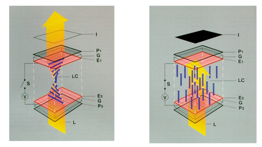
For LCDs, the “on” signal goes to a transparent electrode. Layered above that, you’ll have the liquid crystal material, another clear layer with the opposing electrode, and various polarization films (above and below the whole stack) as well as color filters. There will be a backlight with diffuser below the whole stack. The light shines through the stack, with the liquid crystal material potentially altering the polarization, and in combination with the polarization films, determining whether light passes through that pixel or not, and with the color filter determining the color of each subpixel.
For OLEDs, the “on” signal goes somehow into the OLED material, which is painted (or printed) onto the backplane and then sealed away from the environment with a clear encapsulating layer. The OLED material will glow or not glow. Each subpixel “capsule” contains a different formula of material for the different primary colors.
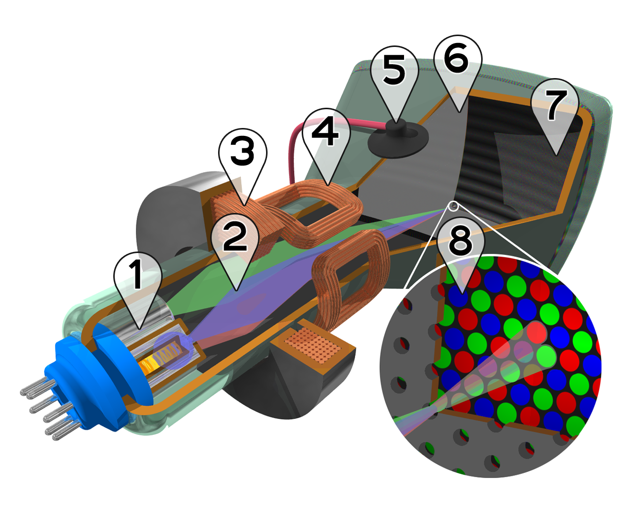
For MicroLEDs, each “on” signal goes to a discrete LED, one for each primary color. Each LED must be cut from a wafer of similar LEDs, then “glued” and wired into its correct place in the backplane. Each LED subpixel will glow or not glow. Each subpixel contains a different material for the different primary colors.
To add confusion, there is the term “miniLED” TV, which refers to the type of backlight used in an LCD TV. Early LCD TVs used cold fluorescent tubes (CFTs), later ones used a sparse array of large white LEDs, and now the latest use a dense array of “mini” white LEDs. What this allows is more precise control of the backlighting, such that where the screen is supposed to be dark, the level of backlighting can be lowered, vs bright areas, where the intensity is raised. This also helps save some energy, since the whole backlight doesn’t have to always be full intensity.
close.
LED’s are big.
Mini LED’s are much smaller.
Micro LED’s are… (you guessed it) smaller still.
energy savings actually come from somewhere else. most LED products on the market refresh (not image refresh, jus the individual LED’s) around 3840Hz. so they are only ON for a super short period of time. (.26 milliseconds/cycle) but shortening the duty cycle, you can end up having the display ON for a decreasing period of time. that can equal less power and less heat generated.
At present, there are direct view LED products all around that you likely see on a regular basis that use any of those types of LED’s.
And in a flagship APPLE store, you see a Sony product they call “Crystal LED” (CLED) that is really just another LED variant.
Source: i work for a direct view (video wall) LED company.
“end up having the display ON for a decreasing period of time. that can equal less power and less heat generated.” … and proportionally less light generated for a darker pixel. The LED does not magically stay of the same brightness, when you reduce drive power.
Energy savings com only from more efficient LEDs
quick lookup says it’s “Just a standard optojunction LED But Smaller” where OLED uses a completely different junction principle and material. the kicker comes from A, making sure they all WORK, and B, reliably bonding those discrete diode emitters to the substrate matrix
The elephant in the room is the cost of this technology. Skipped over by the author conveniently. Maybe in 10 years time it might be worth talking about. In the mean time, OLED tech keeps marching on with brighter, more colourful and more “burn in resistant” displays.
The prohibitive cost of this tech is mentioned several times, you just have to read it.
I’m so sick of OLEDs going blank on our clocks.
yeah, yeah, just unplug them for a few days, and they come back (somewhat).
In these discussions… Micro LED is irrelevant. we see micro and mini being tossed around and from what i have seen, the difference is largely semantics. (yes i know… one is MUCH smaller… but the end results are indistinguishable)
what does matter is;
1. Pixel pitch/resolution. samsungs “the wall” isn’t great because it has micro LED’s… its great because the pitch is .84mm. so this means that a 4k wall would be only 11.29′ wide. most of the market is at 1.26 mm at this point (4k screen is just shy of 17′) when somebody comes out with .6mm, we wont care if it is mini or micro LED. we will care that a 4k screen is only 8′ wide.
2. Brightness… most direct view LED at present is designed for screaming bright boardrooms with direct sunlight… which would melt your eyes at home. so we need a product that is much much dimmer. but can still cleanly reproduce the incredibly subtle nuance of a killer grey scale so that Donnie Darko look s great and you see all the details in the shadows.
Beyond this… the flexibility of LED wins the day. whether its a huge TV in the man cave, out by the pool, as your kitchen backsplash (yes, rich people do that https://www.youtube.com/watch?v=SdCOMmd3OuA ) or even just architecturally integrating them into the environment so that the “wall” that is just white during the day is able to play a sunrise or a football game when you want it to. direct view LED TV’s are truly video Lego.
Source; I work for a direct view LED company.
nano LED
The question I have is, can we even see in 4k?
I did see an interesting youtube video about it.
My father was on a cover of Business Magazine back in the 1980’s when
digital televison was on the horizon, and he told me that each system
has its drawbacks when it comes to a display. CRT had burn-in, LEDS dim
over time etc. Will these LEDS get so small, you’ll need a really powerful
magnifying glass or microscope to see them? At that point will a dead pixel
matter? THe last I heard, over the air tv stations are still broadcasting
in 720p. So, at what point do we no longer see the pixels?
One of the things I’ve been looking into is short throw laser projectors,
what their strengths are, what their drawbacks are…
Every technology is going to have both.
Lastly, if you don’t have good vision, as a lot of older folks don’t, it’s
probably moot. I will be having cataract surgery in a few days.
I had a retina detachment 6 months ago.
I think the holy grail isn’t microscopic LEDS, but if scientists can figure out
how the eye sees. Is it seeing pixels that the brain is converting to a solid
smooth display? I’m no expert, but I can say that if your eyes are not good,
I doubt the number of diodes no matter how small is going to matter.
Your eyes’ acuity is expressed according to an angular measurement, since this is invariant with regard to the distance something is away from your eyes. Therefore, the number of pixels, the size of the TV, and the distance you sit away from it all must be considered in order to answer your question. However, we generally assume that, in ideal situations, people watch TV with it taking up a certain field-of-view (measured angularly). It doesn’t make sense to have a TV so large that you can’t view it all without turning your head side-to-side (assuming regular movies, not IMAX ones). With that in mind, there is a maximum resolution that makes sense. Some websites suggest that this is probably around 4k, with 8k making sense only for more IMAX-like situations.
I think it’s interesting how “organic light emitting diode” caught on. Everyone sees led and automatically thinks light emitting diode rather than light emitting display. And all the companies seem to just go with it.
https://patents.google.com/patent/US8289234B2/en
But when will we see “Free Range” LEDs?
we? i already have them. damn things are everywhere.
Everyone needs to chill with the burn in fear. I’ve had more lcd backlight get sloppy and uneven and flat out die than I ever had burn in issues.
As a data point, I’ve seen many failed LED back lights on cars.
It seems that the biggest problem as others have described is power supply failure.
One would hope that the better manufacturers would add anti-surge mechanisms and make the individual diode blocks
replaceable on a panel using thermal interface material (TIM) or alloy similar to that used for OLED and plasma panels.
I can also imagine a situation where a panel is assembled but can have an individual LED or cluster replaced by spot heating just the bad chip and vacuum lifting it back out, then installing a matched unit from a storage bank.
Calibration would probably be done at the factory with the ability to “juice” really weak emitters for B grade or non critical tasks where a minor imperfection is tolerable.
Even just turn them off in software, a few bad units on an airport sized screen isn’t going to matter for example.
Not to mention the baking hot environment in most cars that end up parked outdoors. The perfect thing for killing any electronic component. Not only do these devices like in car entertainment units need to deal with the heat that they themselves produce, but the fact that they could be at well over 100C right at power on and will have to run for some time that way until the car’s AC can cool down the cabin. And putting a MASSIVE heatsink on things like this doesn’t help either, it’s just longer that the components are going to be at that oven hot temperature until the mass of that heat sink can give up all it’s heat once the cabin cools down.
Compared with the picture of the beamer in my living room, the LEDs do have to be extremely “micro”. A 1080p picture with a width of approximately 3m results in a pixel pitch of about 1,5mm. I think, that is already possible. The remaining question would be affordability.
Yeah, but common, who’s going to spends massive amounts of money on the latest 70+ inch tech just to only have 1080p? If it’s not at min 4K and more realistically 8K by the time it really hits the commercial market, almost no one will buy it especially at the price premium that the new tech will likely have. About the only use of a 70+ inch 1080p panel might be an information board in a public place where they might today have a hub75 style LED wall installed. You’re not really that concerned with the resolution when it’s informational text that people are reading from 30+ foot away. In that use case you’d probably just be better off upgrading to tighter pixel pitch hub75 panels, they already have them today that the pixel pitch is fine enough that at 30+ feet away you’re probably not going to be picking out individual pixels unless you’re a youngster will still perfect eye sight.