The 1980s and early 1990s were a bit of an odd time for semiconductor technology, with the various transistor technologies that had been used over the decades slowly making way for CMOS technology. The 1991-vintage IBM ES/9000 mainframe was one of the last systems to be built around bipolar transistor technology, with [Ken Shirriff] tearing into one of the processor modules (TCM) that made up one of these mainframes.
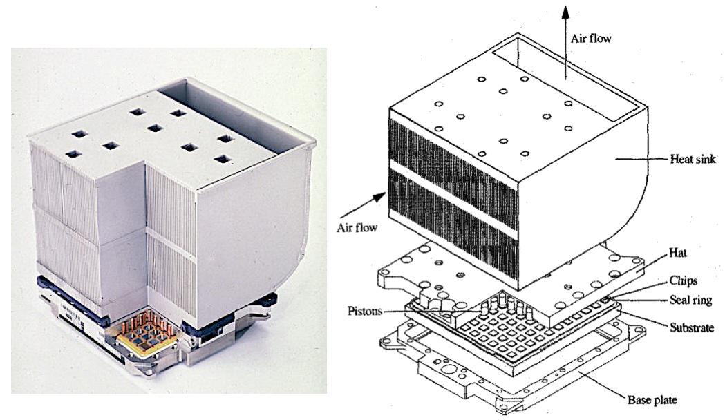
Five of these Thermal Conduction Modules (127.5 mm a side) made up the processor in these old mainframes. Most of note are the use of the aforementioned bipolar transistors and the use of DCS-based (differential current switch) logic. With the already power-hungry bipolar transistors driven to their limit in the ES/9000, and the use of rather massive DCS gates, each TCM was not only fed many amperes of electricity, but also capable of dissipating up to 600 Watts of power.
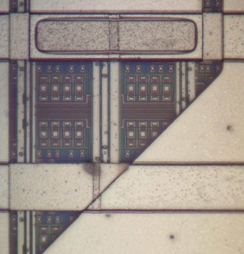
Each TCM didn’t contain a single large die of bipolar transistors either, but instead many smaller dies were bonded on a specially prepared ceramic layer in which the wiring was added through a very precise process. While an absolute marvel of engineering, the ES/9000 was essentially a flop, and by 1997 IBM too would move fully to CMOS transistor technology.
Over the years we’ve featured a lot of [Ken]’s work, perhaps you’d like to know more about his techniques.


Was wondering when this would show up (I knew he requested a few dies from Dave Jones a while back.)
And now we live in a world of chiplets. From CPU to GPU.
https://www.tomshardware.com/news/amd-gpu-chiplet-patent
I worked at a supercomputer startup in the late 80’s and early 90’s. We had an advanced version of these which were a) ECL, b) liquid cooled, c) put die on both sides of the substrate, d) had both interconnects direct from the die to the substrate (think BGA on the bottom of the die) and bonded wires . and e) had multiple substrates assembled into bricks.
Where this has hat & pistons, we had a top plate (titanium) with at least 4 nozzles per die to move Florinert over the die.
Each brick had monster power connectors (~1″ silver pin for each major power bus) and a high density signal connector with, iirc, over 8,000 pins. Bricks were inserted and removed with a small hydraulic fixture screwed into the front. I don’t remember how much power each brick could dissipate, but, safe to say 600W was more than an order of magnitude in the rear view mirror.
A flop? I don’t recall that being the case. I do believe IBM sold a LOT of the ES9000. The reason that IBM went to CMOS was related to technology, not the market for the machines. by going to a CMOS offering they were able to get multiple CPU’s on 1 TCM. Also, I think the picture of the heat exchanger was from the follow on CMOS machine. The Bipolar TCM’s were to hot I believe to be cooled by forced air through a heat exchanger.
TCM’S on the ES machines were all water cooled.
The electrical and mechanical technology to power and cool these devices are the most interesting part of the package.
The saga that Dave Jones went though to get a few dies off is a testament to the fact that the engineers at IBM designed the thermals well!
I worked for IBM in 1979 in the large systems engineering division, retiring in 2017.
The TCM technology was first used in the 308X of the IBM System 370 series.
This was major leap in technology from the previous generation of mainframe equipment.
The technology used in the 308X, 309X, etc systems. They were hardly a flop. I fact they were a major change in mainframe advancement.
Even almost 40 years later I remember being impressed of what the IBM development engineers designed, built and deployed successfully.
These machines truly were amazing.
Worked on most of the above for decades.. ES was hardly a flop and is still an engineering marvel.. its legacy runs 90% of all banks in the world.. and lots and lots more… nothing still like it