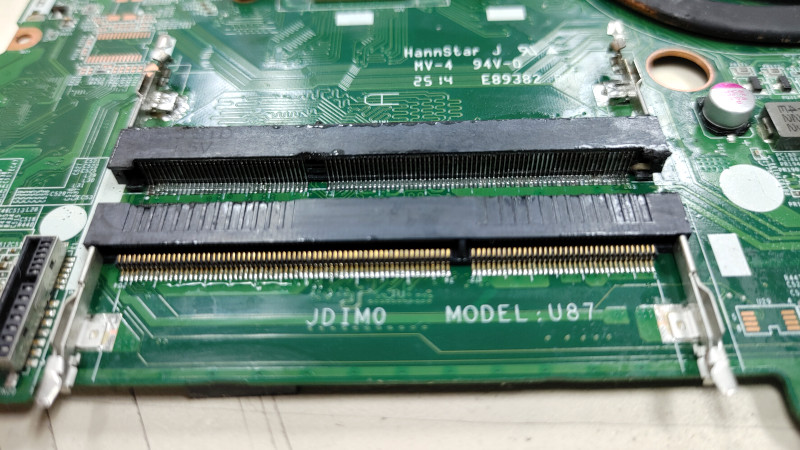
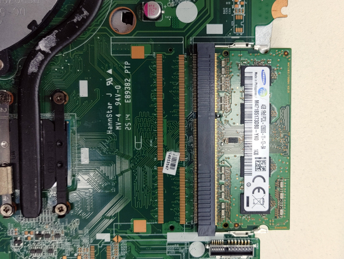
Finding unpopulated pads on a circuit board is often a sign that the device in question has some untapped potential. These blank spots on the board could be left over from features or capabilities that were deleted from the design, or perhaps even represent an optional upgrade that wasn’t installed on this particular specimen. So we certainly understand why [d0rk] was fascinated by the empty SO-DIMM footprint he recently found on a laptop’s motherboard.
The budget Celeron machine shipped with 4 GB of RAM installed in its single socket, a situation [d0rk] hoped he could improve upon with the addition of a second module. But could it really be as simple as pulling the socket from a dead motherboard and soldering it into place? Would other components need to be added to the board? Could the BIOS cope with the unexpected upgrade? There was only one way to find out…
At first, it seemed like the patient didn’t survive the operation. But a close look uncovered that the power button had actually gotten damaged somewhere along the line. Once [d0rk] fixed that the machine started up, but unfortunately the operating system didn’t see the extra RAM module. Even after upgrading the BIOS, the computer remained oblivious to the additional memory.
When he went back in to inspect his solder work for shorts or bad joints, disaster struck. For reasons that aren’t immediately clear, the computer no longer starts. Even after pulling the transplanted SO-DIMM slot off the board entirely, [d0rk] says it won’t make it through the self-test. Obviously a disappointing conclusion, but we respect the effort he put into the attempt.
While this memory upgrade didn’t go according to plan, we’ve seen enough success stories over the years to balance it out. From old wireless routers to cutting-edge video cards, plenty of gadgets have received a memory boost courtesy of a soldering iron and a steady hand.
[Thanks to Timothy for the tip.]


A lot od the time the bios will limit the max ram on these budget machines for instance I have a dual core Celeron tix board with 2 sockets but the most it can handle is 2 gigs a socket and putting anything larger grants you a no post
Cant make it cheap AND upgradeable… That would cut into future sales
If you want to make the machine work with an extra slot, your only real hope is to port Coreboot to it.
From those familiar with the workings of Coreboot, during ram init the SPD lines for detecting the DIMMS must be specified. These circuit-board-specific (like all GPIO lines) and are told to whatever is doing the ram training. Coreboot for some families has native ram init code, but more commonly now uses intel’s memory init blobs like the FSP or mrc.bin.
It’s the specification and handling of these board-specific lines that’s one of the hardest parts of porting Coreboot to a new motherboard, because it typically has to be guessed at or electrically traced out.
Best case scenario otherwise, the GPIO lines for the additional SPD are un-configured, never scanned, and the corresponding slots are uninitialized and don’t interfere. Worst case, the RAM code bugs out or the unconfigured slots interfere and crash the BIOS during the ram stage.
All of this assumes, by the way, that all of the electrical connections/modifications are 100% sound.
The board may have various termination resistors that are populated but the wrong value for two ram slots, for example. Or god knows how many other issues. You’d have to ask the engineer at compal or similar who designed it. At the very least you’d want the schematics for both versions of the board for comparison, and probably the boardviews too.
Agree on the components that are used on the mainboard.
The availability of some resistors and their values are also used as advanced DIP-switches to signal a certain configuration to certain hardware components and BIOS. Based on that, certain features will be available and other nots.
However, does this Celeron CPU actually support 2 memory slots?
Beins a budget processor, most (almost all) Celerons only support a single memory slot (with 2 channels). (Which is confusingly something completely different as “dual-channel” RAM.)
The same basic mainboard can be used for other non-Celeron processors and in that case the 2nd RAM slot will probably be populated.
A lot Celerons have reduced memory controllers, so it might be the CPU doesn’t even have the pins that the second slot relies on. Celerons are just Pentium chips that failed certain wafer tests, the failed part of the chip is still there but disabled, and it isn’t rare for companies to still keep the pin and lead in place, but just mark it as “DNU” on the datasheet. So maybe by adding the extra RAM module slot, they inadvertently powered up the failed controller enough that its power fuse was reset and now the CPU is trying to bring up a failed memory controller during boot.
Or my other thought is that the soldering heated up the board enough that some of the inner layers warped and some traces got damaged.
I would have started with slot A or JDIM1 instead of JDIM2.
It’s nice to see a failed attempt at this.
Not because it failed, but because so many others fail. The internet is full of hacks that worked because the ones that didn’t rarely get posted.
The reason the hacks that worked were found is because people tried thousands of things like this and failed over and over. It can be a little disheartening to people who are new to hacking hardware to see others make it look easy and then find it to be a minefield. This is a good reminder, it doesn’t always work out, but it’s always worth a try.
Failure is a part of learning, where would we be if the first man to lap a flint knife just gave up because he hit his thumb?
As they say, you learn far more from failure than success,
“Up from the ashes, up from the ashes, grow the roses of success!”
Admittedly I failed to see the amusement of the, Caractacus Pott, reference as a young child.
I know there aren’t many fails of the week posts but surely this is one of them.
sometimes you gotta have the nerve to roll the dice – it can potentially change the course of your life
Bought the Macintosh 128K as my second computer – thinking that this was really swell because it had twice as much memory as the Commodore 64 it was supplanting. But wasn’t long before I discovered it wasn’t good for much more than doodling in MacPaint. In the era before Internet I came across a document (probably from local Mac user group) that instructed how to perform a self-upgrade of the 128K Mac to a 512K Mac.
So I decided to go through with it. Ordered the denser memory chips. Bought some de-soldering braid, grabbed the soldering iron. First job was to de-solder all the existing memory chips, solder in sockets, then solder on a bodge wire to the mother board, seat the new chips, and power it up. Lucky for me it worked perfectly. I now had a rather usable Mac 512K.
Got an external hard-drive, Lightspeed C compiler, MacsBugs monitor, the Mac Toolbox documentation from Apple, and started to really learn the craft. Shifted over to taking computer science courses to compliment my self-taught, seat-of-the pants efforts (and helped that a good buddy and fellow Mac enthusiast was already a grad student in CS).
First paying job was programming Macs on a team of 2 software devs and the rest a bunch of EE geeks – but we all shared a great affection for the Motorola 68000 – and they would let me borrow their Logic Analyzer to pin down memory stomping software bugs on the Mac.
Went on to work for major software companies and so on. A most rewarding career shift.
All because I rolled the dice to take soldering iron in hand and do my own memory upgrade of a Mac 128K.
So in a back handed sort of way – thanks Steve Jobs for being so bull-headed stubborn on shipping a Mac with way too little memory to be practical
I absolutely love this story, thanks for sharing! Would love to see what you can do now days…
Probably get sued by the manufacturer for using ‘their’ device the way you want ed to and paid for. Probably give you some garbage about IP theft.
“see what you can do now days”
My latest hobby in recent months has been flashing cell phone ROMs with forks of Android 11 (LineageOS) that are completely de-Googled of Google’s apps and services (uses microG in place of some GApp services so that most – probably 90% or so – Android apps can still run fine).
So, yeah, my thing these days is looking to shed reliance on Bay-Area Big Tech company software intrusions – they’ve all gone to the dark side – and that’s not being tongue and cheek (I used to work for one of them and really saddens me – but guess is not surprising how they’ve collectively turned out).
Therogerv – i’m looking to de-google my phone too. Are there any good websites you recommend?
Otherwise i’m gojng to have to roll my own phone with a raspberry pi and 4G module. Which would be _way_ more work, but definitely fun….
Don’t forget the extra mux chip you had to add to provide the additional address line. (I did that upgrade too.)
You could also stack extra memory chips on the existing ones, with one leg (CS) sticking out from each, all wired to yet another address line, to double the ram from 512KB to 1MB. Did that one too!
I had a Mac 512KE that someone had fished out of the garbage. What I found interesting was that it had a little board with a multiplexer that plugged into the main board. I never compared it with photos in the Dr. Dobbs article about the Fat MAC, but given the tiny board, it almost looked like the Mac 128K was designed for 512K, or designed for upgrade ability. Why else have the pin in a neat little row? If they redid the board for the 512K, why not put the multiplexer on the main board?
Don’t forget about the original xbox.
IIRC, only a few games actually utilised the extra 64mb of RAM, so although the upgrade technically worked, it was kinda pointless doing it.
The extra DDR was for development work. If you bother to run Linux, it could use the extra RAM.
Could it be that the CPU that’s installed does not support the second channel?
It’s 99.9999% certain that the BIOS doesn’t know it’s supposed to scan the SPD lines for the 2nd slot. It wouldn’t be compiled with support for a 2nd slot. All of this is very, very board-revision-specific. Working out all of the GPIO lines and how they need to be twiddled is one of the hardest parts of porting Coreboot to a new motherboard.
Before you could port Coreboot to the board and try to get it right though, you’d need to be 100% sure that the modifications are electrically sound in terms of termination, etc.
Getting those GPIOs set up, the routing handled, and other board specific porting work can be problematic as an OEM with BIOS engineers on staff. tying to reverse engineer everything to create custom firmware sounds like a small nightmare.
Hacked On SO-DIMM Shot Was Worth A Slot
Having worked with this stuff for a few decades, both on the hardware and firmware side, this hack was a good start, but fell short where it counted. The reverse of the board probably had a lot of passive components that had to be populated for the thing to work right. I bet the VREF_DQ needed a few passives, and there’s probably a DIMM-specific cap-farm for all the various supply pins. Plus the ODT lines probably need resistors. Finally, some boards don’t hard-code the address, but do so via resistors that tie the SA0/SA1 lines to either ground or supply. Just doing the VREF_DQ, ODT and SA0/SA1 might make the thing work. Some comparison between the board and either the actual schematic, or just a reference design schematic for the chipset will probably point out what’s needed; all available through internet searches for those daring enough.
Once all that is done, the BIOS side is almost certain to work, because it’s easier for the firmware folks to make one version that looks for all available DIMM configurations, rather than customize them per marketing model.
I suspect this is probably right. If they’re not gonna bother making a whole new PCB for this model, just leaving stuff unpopulated, I doubt they’d bother with writing a specific BIOS for this one revision, but one that works for all models using this board in its various hardware permutations.
I looked at the back of the board, and was expecting a mirrored set of missing components or something for the second slot, but maybe they would be interleaved due to the close proximity of the slots?
Images of the back of the board https://imgur.com/a/yP6bVHb
The good news is that the bypass cap farm is in one place, so that’ll probably be good enough. The bad news is that you are looking for a few good R’s to place. With a schematic for this board it’d probably be pretty easy. Looking at this it’s not immediately clear where you want to go, except to trace out the critical VREF pins and ODTs. On the upside I don’t see any obvious SA0/SA1 type selection point anywhere, so that’s presumably hard wired.
And the reason the board stopped working was probably excessive thermal load causing a trace failure. If the board is for fun-type testing only, I use a low-temperature bismuth based solder that melts at a much more board-friendly temperature. The downside is that the solder is far more prone to failure over time.
It’s been a while since I’ve worked in that industry and the early boot stuff was not my specialty so I’m almost certainly missing details.
In general BIOS IBVs and OEMs just generally stick to the Intel reference BIOS. But when I look up the part number of the board, it looks like it’s made by Quanta for HP, and HP is a strange beast in that they will put in at least some effort to lock down some aspects of their machines (though it’s hard to say what until you actually run into the lock outs).
With this board, the best I could do is guess. But IIRC the mobile BIOS should be from one of the two main BIOS IBVs so someone may have already invested some time into hacking the BIOS. But their enterprise PCs may still be using an in house BIOS core (a hold over from their agreements with Intel around Itanium).
My point is that their is a lot of in house knowledge to allow for a lot of customization and, at least in the US, the BIOS engineering world is pretty small so it’s likely there is some side channel knowledge transfer between engineers in different divisions of the company.
A blog post i saw a while back (https://medium.com/@p0358/removing-wlan-wwan-bios-whitelist-on-a-lenovo-laptop-to-use-a-custom-wi-fi-card-f6033a5a5e5a) linked to a fairly neat tool https://github.com/LongSoft/UEFITool which appears to be a tool to edit/modify EFI images.
Dunno about a HP laptop, but it happily picked apart the efi image for the gigabyte motherboard in my desktop.
I’m sure there are companies that have in house devs for specific stuff, but I’d guess a lot of EFI images are generated from premade modules that insert hardware specific values from the board manufacturer (memory maps, io pins,etc) into a lego-esque built rom.
Thank you! I thought the model number looked a bit familiar. In fact I have the schematics for this board, a HP 15N made by Quanta. The parts that need to be populated for DIMM1 to work are R260, R264, R263 R265, R266, R274 R270 and R269. There’s a bunch of caps, too, but with the R’s you’d get close enough to see if it works.