The MOS Technology 6502 CPU was a popular part in its day. In various modified versions, it powered everything from the Commodore 64 to the Nintendo Entertainment System, and showed up in a million other applications too. A popular variant is the 65C02, and [Jürgen] decided to whip up a pin-compatible FPGA version that runs at a blazing 100MHz.
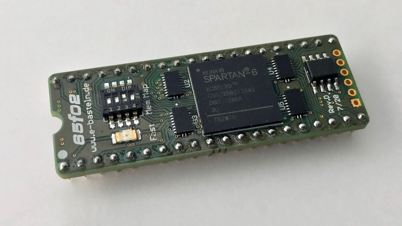
The CPU core was borrowed from work by [Arlet Ottens] and extended with 65C02 functionality by [Ed Spittles] and [David Banks]. [Jürgen] then packaged that core in a Spartan-6 FPGA and placed it on a small PCB the size of the original 65C02’s 40-pin dual inline package.
The FPGA is set up to access the external CPU bus with the timing matched to the clock of the host machine. However, internally, the CPU core runs at 100MHz. It copies RAM and ROM from the host machine into its own internal 64 kilobyte RAM, minus the areas used for memory-mapped I/O by the host. The CPU then runs at full 100MHz speed except when it needs to talk to those I/O addresses.
It allows the chip to accelerate plenty of tasks without completely flipping out when used with older hardware that can’t run at anywhere near 100MHz. The pin-compatible design has been tested successfully in an Apple II and a Commodore 8032, as well as a variety of vintage chess computers.
We’ve seen the opposite before too, with a real 6502 paired with a FPGA acting as the rest of the computer. If you’ve got any cutting-edge 6502 hacks of your own (not a misprint!), let us know!
[Thanks to David Palmer for the tip]


Awesome! Now how do we slow this thing down….
Jane!!!! top this crazy thing!
And how do we over clock it.
It has an “automatic real-time mode”.
This detects certain addresses, and for functions that are timing sensitive (sound generation, casette interface, etc) it uses the slow speed.
http://www.e-basteln.de/computing/65f02/65f02-details/
The rumor mill says Spartan-6 will or has become unobtanium, so that would stop it pretty quick.
Everything will become unobtainium at some point… ;-)
For the time being, the Spartan-6 family are active parts. They “just” have 52-week lead times like, unfortunately, so many other ICs from various vendors. Life as an electronics hobbyist was better before the Covid-induces semiconductor crisis…
Does it run Doom??
I really need this back in 1984, when I wrote a simulator that took weeks to produce results on my C64. :(
Kontron sold a full-on 6502 emulator and debugger back in the day. It was in a big box with a ribbon cable to the DIP connector. It cost more than a college education but it did the job if your boss could afford it.
Hence my site’s motto “Solving yesterday’s problems today.” ;-)
Where do we buy said 6502 chip?
“This is a hobby project, and I have no plans at the moment to take it commercial.” e-basteln.de/computing/65f02/65f02/#status-and-next-steps . I wonder if hackaday is trying to nudge some “maker” into producing it, it seems to be completely Open Hardware and Open Software. And I think there should be tremendous interest in the vintage computer community beyond “old chess computers”. But maybe it’s too big a project to take on in the “chip-shortage” environment of today? It’s the 40-pin compatible output that interests me
Unless you are asking for the original. You would be much better off trying to find a WDC 65C816, which were used in the Super NES, maybe on eBay.
Also, if commercialized, I’m sure people would make their own “retro” computers with it. Nice work.
With a little HDL, the same hardware could probably synthesize a WDC65C816. It would be interesting to see.
The link to the source code is not working.
You can buy the W65C816 CPU’s from Mouser Electronics.
Hmm, would love someone to take all the “new retro replacement” ic’s and build a system with it, like the supersid for sounds, picoVIA for io, this as a cpu etc.
Could you give more information on these? Googling supersid, and picoVIA gives results not really related to C64 so I’m sure I’m not finding the right things.
Commercial 6502 FPGA is available from WDC
I wonder if it is more stable than Zip Chip… ;)
I hope so. And gets more hours before failure.
This sort of thing existed in the past, a plug in accelerator. Same premise, built in memory so the whole thing can run fast, except when doing I/O. But too expensive for me.
This seems to be smaller, and does it by other means.
I’m not clear what you are talking about. FPGAs being too expensive generally? “Plug-in accelerators” being too expensive? Too expensive compared to this completely open source, open hardware project?
Certainly Amiga accelerators like the Vampire1200 V2 can go much beyond a 68060 200Mhz (which was an “accelerator chip” in the past) to something like four times as fast. http://www.apollo-core.com/v1200.html But I’m not certain that’s what you are talking about.
One of the issues with re-implementations of vintage 6502/65C02/6509 computers is that on many, like the Apple II series, the timings are complex and overly dependent on the CPU. The first Apple II’s can’t even adjust to a 65C02. Trying to adapt the system, or a new hardware emulator, to anything like 100Mhz is impossible. I think there’s limited use, in Apples for example. Better not to use a FPGA of just the CPU alone, but also putting the sound, the 80-column text card, and a great deal more in FPGA as well.
I’m talking accelerators 30 years ago. They existed, I didn’t pay attention because they were more than I was willing to spend, and I’d moved onto the 6809.
The posting here seemed to present it as a new thing. The implementation is new, but the concept isn’t.
My co paid $11,000 for a 6809 emulator back in 1992
The 65F02 does work nicely in the Apple II. It respects the Apple’s 1 MHz bus timing, including the interleaved video RAM access. It can also automatically slow down program execution to the original speed in timing-critical code sections. The latter will not work 100% with all coding patterns, but it certainly works for speaker beeps, reading the paddle inputs, and reading/writing disks under DOS 3.3.
My project web page has some details about that. Feel free to read it before making further assumptions. ;-)
Excellent project, Jürgen.
Now how about the rest of a computer that can keep up with it?
Well, the whole idea of this accelerator is that the existing host computer can be used without changes.
The host’s RAM and ROM will be replaced by the fast on-chip RAM in the FPGA, and hence don’t affect the operating speed at all. And the host’s peripherals will continue to operate at their designed (original) speed, with the 65F02 automatically slowing down to access them.
Amazing. So much of the original ROM and DOS depended on the clock functioning at a precise speed and DMA to hardware…. Great job!
[quote]”I think there’s limited use, in Apples for example.”[/quote]
We have lots of members on the 6502.org forum who are building their own hardware; so although a few users might be interested in putting it in an Apple, I mostly envision this being used in new designs.
A 6502 FPGA core – ugh. Just because it can be done doesn’t mean it should be done.
Heh, I think you might be on the wrong website. You just described one tenet of the hacking ethos.
A electronic etch-a-sketch. Make all the forbidden designs one wants, then invert and shake and all the incriminating evidence disappears. No one will know the depths of depravity reached.
What’s wrong with such a core? Not one I know anything about, but its of the age when its usefully functional but simple enough to actually understand, seems like great core to use if you want to.
If you need a real but small 8 bit CPU core on an FPGA (a soft microprocessor), 6502 or 65C02 is actually a great choice for the same reason it competed well against the 6809 and the 8080/Z80: its minimal, yet useable feature set gives it good bang for the buck. Instead of the minimalist design choices saving money on a cheaper CPU ASIC, though, it saves on LUTs in an FPGA. And not only can you find the soft core implemented already online, the legacy of the 6502 means you’ll have a relatively easy time finding suitable development tools to write the software of firmware for it.
Not that there aren’t alternatives. Picoblaze, for instance, if 8 bits is enough. Supposedly, someone somewhere actually decided on and implemented a BrainFuck soft core to run some, presumably rather simple, programmed logic in some (commercial) application they couldn’t specify. It doesn’t get lower-footprint than that.
Millions of 6502 core equivalents are manufactured every year, for better or for worse.
more like tens of millions. WDC was saying only a few years ago (five?) that it was over a hundred million a year; and in a recent interview, Bill Mensch, the owner and president, said, if I understood and remember correctly, that they were going to be going into labels on things like beef, fish, and chicken in the supermarkets, dramatically increasing the production numbers of 6502’s.
Oooh. Gotta make one with a couple tweaks!
This could make my Battlezone a bit tricky to play, sped up by a factor of 66….
But I think I’ll be up to the challenge!
Apparently standalone chess games have seen a lot of testing of this device. That makes sense, speed up the computer side.
Yes, yes, this is all well and good, but what here out there will finally emulate a Spartan6 with a room full of 80’s era microprocessors!
Put one in a C64 and one in a 1541 disk drive, faster data compression over dog slow serial line. Theoretically more data could go through via compression
The C64 used the 6510 chip. Would the 65f02 work in it?
It can be configured for various computers, to account for where the I/O goes. So there us some level of adjustment. Whether an I/O port and the insgructiins for it can easily be added is another question.
You read my mind on that one.
And just because you can comment doesn’t mean you should comment…
Ugh, thanks for that, wordpress!
U R Welcome!
B^)
Impressive!
Would love to see that as a 65816 with a few MB linear memory on the chip.
How does that memory copy concept work for machines with dedicated graphics chips like the Atari/C64 that can vary where in main RAM graphics come from?
The 65F02 will need to know about the host’s bank switching mechanism, and duplicate it inside the FPGA to keep track of which RAM to use in which address space. Quite feasible, I have implemented a basic version of this for the Apple II.
The bigger hurdle is the limitation to only 64 kByte RAM in the FPGA, which means that systems with more than 64k total RAM+ROM can’t be fully accelerated. The Spartan-6 I am currently using is not available with more RAM in the compact BGA package I need. I am pondering a 65F02 rev. 2 with a more powerful FPGA, and will probably not tackle support for further home computers with the current version.
Nice job!
Many thanks! Is that you, Arlet, the author of the original 6502 core I used? If so, even more thanks (again)!
Yes, it’s me :)
VERY NICE !!
WHERE DO I GET ONE TO TRY OUT WITH FASTFINGERS?
Now I want a Z180 version of this…..
The Atari 400, 800 line had a custom 6502 (called SALLY) as described below. Has this capability been included in this FPGA chip?
In contrast to the MCS6502 and equivalents, the SALLY 6502 has the addition of
a /HALT signal on pin 35. The SALLY 6502 also has a second R/W signal on pin
36 (in addition to pin 34). Pins 35 and 36 are not connected on the MCS6502
and equivalents.
Those pins are connected in the 65F02, but are used for programming the FPGA via a built-in USB bootloader. They could be re-purposed as /HALT and R/W in the FPGA’s runtime configuration, but lack the level converters to 5V. Would probably still work, but it is not a clean solution.
I am considering a rev. 2 of the 65F02, which would use an FPGA with more on-chip RAM (to fully support bank-switched systems with more than 64k total RAM+ROM), and bi-directional level converters on all pins (to support variations like the 6510 and SALLY). That’s probably what we should wait for before diving into support for further home computers beyond the CBM/PET and Apple ][.
Sounds great. With more RAM a 65816 would be great, too.
The ‘816 offers a ton of benefits even in situations that have only 64K of memory space.
With more memory a 65816 could use linear (bank register) memory on almost any machine. All its other extra capability would work on 64K as well, of course (even though I find it quite difficult to wrap my head around keeping track of the register size changes when programming).
slx, I’ve used it for Forth. I leave the accumulator in 16-bit and the index registers in 8-bit almost full time, very seldom changing them. I’m in contact with another user who has a different application who does the opposite, leaving the accumulator in 8-bit and the index registers in 16-bit almost full time, seldom changing them. The REP and SEP instructions are awfully cryptic though, so I use macros with friendlier names, ACCUM8, ACCUM16, INDEX8, and INDEX16. Another user I know called his SHORTA, LONGA, SHORTI, and LONGI, IIRC.
Back in the early 1980’s, a hardware engineer and I built a PDP-11 hard card for the Apple][ that had a T11 chip, 32kb of RAM, and some PALs for the Apple bus interface and DL serial port emulation. A program running on the apple provided a pass-through for one of the DLs to a serial card in another slot or emulated a TU58 using the Disk][, and emulated a VT52 on the screen. It could boot a small RT-11 image from the TU58 without modification. We were hoping to add an additional 32kb RAM with bank switching of 8K for the IO. The bootstrap instructions were written to RAM by the PALs. This had been inspired by the z80 hard cards that were being sold for the Apple at the time, and we thought that it might be useful in labs and such.
I wonder if something like that could be added alongside the 6502 core on one of the larger Spartan FPGAs. Not much practical use today, but would be fun.
is anyone workinworking on a 400m400mhz z80 replacement please
rogerjowett@gmail.com
400mhz
So, one clock cycle every 2.5 seconds?
I think you mean 400MHz.
That’s not so easy to achieve with FPGA especially with something like the Z80 which has a very complex timing scheme.
The 6502 has a symmetric and linear clocking scheme.
If you abandon the Z80s peculiar clocking scheme (it was mostly done that way to refresh dynamic RAM) and aim for a cycle incorrect implementation then you would loos a lot of complexity and cost.
Then there is the second problem. The 6502 is very RISC like and the Z80 is definitely CISC.
Pushing the Z80 past 50MHz will require a lot of extra gates and a good clock domain scheme.
How many extra gates?
Well something like the RISC (like) 6502 doesn’t have a lot of different data paths so it’s easily sped up with some extra gates.
However the Z80 (CISC) has many internal data paths and would require many extra gates. Even then the Z80 also has a lot of indexed modes which would become a bottleneck and probably THE bottleneck that limits the overall achievable speed.
well I only puked the number 400mhz for the z80 as that would be equivalent to the 100mhz of the 6502 no? c64 had 1mhz 6502 zx spectrum was 3.5mhz but 3d graphics were definitely faster on the spectrum
piked
But wasn’t the clock in the Z80 divided by four? Internally it wasn’t clocking faster, but the design needed a faster clocko
all I know is that the ula slowed down the processor when it accessed video ram
Thanks for the comments on a potential Z80 version, RÖB.
For fast code execution from internal RAM, being “cycle exact” should not matter at all — it’s invisible to the external host computer anyway, and decoupled from its clock. For external bus cycles the FPGA would have to respect the exact host timing, but these are slow anyway. So I think there is room for a streamlined Z80 implementation.
To implement the more complex instruction set of the Z80, there are certainly plenty of unused logic cells in the FPGA. And routing delays within the CPU logic are probably not going to be the main timing bottleneck. The most time-critical path inside the FPGA is to the RAM and back: Since the RAM is organized in blocks which are distributed across the whole chip, some routes are really long.
In any case, a Z80 version would require a new PCB design. While the FPGA pins can of course be configured flexibly, the 5V level converters are hardwired as inputs or outputs on many of the DIP-40 pins. And the +5V supply and GND pins are hardwaired as well.
if the 490mhz z80 is possible is 800mhz video also available?
Not sure what you mean by 800 MHz video. The pixel clock? But in general — no, this plug-in CPU accelerator does not deal with any peripherals. They all stay exactly as they are in the host computer.
(And no promises on a 400 MHz Z80! The devil is in the details, and RAM timing is one of them; so the effective speed of a Z80 FPGA core with on-chip RAM might be well below 400 MHz. And I’m afraid I don’t have the time to look into a Z80 version at the moment.)
ok well thanks anyway
https://youtube.com/shorts/Z97sN0luei0?feature=share
I have something z80ish in the works. Not 400MHz, but I think I can do 270MHz…
ths incredible would it work in a zx spectrum?
Wow, I have to pry!
270MHz is as far as I thought you could take this with FPGA. Are you using something that us common people can afford? A lower end part that just has enough gates and BRAM?
I can see a pipeline here? Four stages? Are you abandoning the refresh perhaps apart from the “R” register?
I’d like to do something like this but I don’t have time and I can’t decide “how much” compatibility. So many undocumented instructions that I would probably support and then there are undocumented instruction extensions that I probably wouldn’t bother with.
I must admit I’m being disingenuous here, sorry. I’m using a Pico overclocked to that speed (the maximum it can do while still being able to access USB and flash without extra wait states), it’s not the speed of the emulated Z80.
I’m not focussed on boosting execution speed anyway, the primary goal is perfect emulation (including R, I’m leveraging flooh’s chip emulator library) while adding USB device support and ram expansion. I’ll set up a special configuration that accelerates code in local RAM but it’s not a primary goal.
Cool project. I wonder how the speed compares to my emulated 6502/6510 drop-in processors which use a Teensy 4.1: https://microcorelabs.wordpress.com
That will depend very much on the programming of the Teensy. I think that with your current Arduino implementation the Teensy is quite a bit slower than the 65F02. But there is probably a lot to be gained with an optimized emulator implemented in assembly code.
The only way the Teensy approach is at all feasible is because it’s clocked so ridiculously high – 800MHz, yikes! Almost all of that speed is needed just to get an acceptable latency in the bus transactions; otherwise even the simplest response to a clock edge takes most of the clock cycle to accomplish.
I’ve seen it done on a rather more sensible M4 microcontroller, but that implementation isn’t cycle accurate – bus transactions are bit-banged blindly and then the bus sits idle for a cycle or more while doing the actual emulation and other bookkeeping. Fine if what you’re running isn’t too timing sensitive, but it would break some games and most demos, given that they often rely on carefully calculated cycle timings.
For the 65F02, accelerated operation (at 100 MHz, operating purely from internal RAM) and real-time operation (either to access I/O ports in the host computer, or to run timing-critical code at original speed) are two entirely separate matters.
In accelerated mode, cycle accuracy does not matter at all — although the 65F02 is actually cycle-accurate in 100 MHz mode too. When an I/O address is accessed, or when the 65F02 has deterrmined that timing-critical code related to I/O operations is being executed, the speed falls back to the original host speed, and timing and cycle counts do matter.
I could see this working alright with a microcontroller instead of an FPGA. When serving the external host bus (for I/O operations), you have all the time in the world to wait for the clock edges and drive the bus, since that bus operates at a leisurely pace.
The Cortex-M7 on the Teensy 4 does not look so unreasonable to me. 100 mA at 3.3V, so 70 mA at 5V with a switching regulator. The chip is less expensive than my Spartan-6 FPGA and has a smaller footprint, even more so when you include the required power supplies. I don’t think it is overkill…
What are you designing around the Z80? Any documents online yet? Just curious…
The M7 is at the extreme end of present-day microcontroller speeds. Very few run more than 200MHz, and it’s only a small segment of embedded uses that really need more power than that – normally things move over to an application processor and run Linux or something beyond that point for raw compute speed and add a modest uC for any remaining hard realtime requirements.
That “leisurely bus speed” you think gives all the time in the world is incredibly deceptive. The gotchas mount up really fast – firstly ARM interrupt latency is a minimum of 12 cycles from a trigger before application code starts executing. Abandoning interrupts for halting the processor and resuming on trigger instead only brings that down to 6 cycles. ARM instructions are also all multi-cycle, so even a tight “read a GPIO repeatedly until it changes” loop takes a dozen cycles or more.
The Z80 clock is 4MHz, which means there’s an edge every 8MHz. For a pretty speedy 168MHz clocked Cortex-M4, that’s only 21 ARM cycles per half Z80 cycle, half of which is already lost just synchronizing to the edge, and the rest is eaten up by even the simplest processing. That’s long before you even think of running the emulation code! Even harder is that on the Z80 there’s a /WAIT signal to pause execution that needs to be handled at the cycle level, but there’s already no time to do it.
6502’s bus may be easier to handle, I don’t have the experience to say. But it’s still going to need more ARM clock speed than one would expect.
As for the z80ish project, there’s nothing online yet (heck these comments are a bit more than I was intending to reveal at this time.) I don’t have a working prototype yet, so there’s still a decent chance I’ll hit a brick wall.
My current design relies heavily on a Raspberry Pi Pico, as the PIO state machines it has are critical to avoiding the timing problems I mention in my other comment – I can delegate the bus transactions to programs running on those (which can do single-cycle GPIO reads/writes/waits) while the ARM is mostly free for emulation/USB/etc. Even so I’m really pushing the limits of what the PIO was intended to do.
Thank you for the detailed comments, pelrun. Seems that I cannot reply directly to your comment — is there a limited nesting depth in this comment section?
I agree that serving the 8 MHz bus for a Z80 system is pushing the limits for a microcontroller-based solution. Using the state machine units in the RP2040 is a clever way to deal with that. I hope that it can be done in software with the fast i.MX RT processor on the Teensy, but have obviously not proven that yet. My main interest is the 65xx family, but I would like to support 5 MHz bus clock there, so not too far away.
To serve host signals like /WAIT or the 6502’s corresponding RDY, or interrupts for that matter, I was considering interrupts on the i.MX RT to avoid more polling in the main emulation loop. Again, ab unproven idea so far.
I’d love to see what you can squeeze out of the RP2040 — best of luck with your project!
Yeah, five levels deep is all we get on HaD :)
Could you please post a video to demonstrate how fast the 65F02 is? Or at least a picture of your board inside of your Apple II running something/anything? The links to your code on your website dont work either, so without any videos, pictures, or code we can only take your word that your 65F02 is faster than anything or if it even works at all.
Sure. You already asked the same question over on 6502.org, and I just posted a link there. I wouldn’t have minded you taking my word though…
I saw it. Very nice! You should post the link here too!
in the 80s there were already chips that replaced the original 6502 there were several solutions the 65F02 reminds me of the zip chip. is there any intention of producing it?
Wow — I had never heard of the Zip Chip, but having looked at it now, I am impressed! Amazing packaging density for its day, and a 4 MHz or 8 MHz 6502 was quite nice indeed in 1986. Here’s a photo of the Zip Chip sans enclosure:
https://www.applefritter.com/files/ZipChip4.jpg
I’m afraid I won’t have the 65F02 produced in quantity. Just too much hassle with compliance, production and test, distribution — and now the chip supply bottlenecks on top of that. Xilinx’ delivery time for the required Spartan-6 FPGA is more than one year…
Juergen, it’s been more than one year since you replied. What is the status of your project, now that it is the end of Dec. 2023?