
For most of human history, our inventions and innovations have been at a scale that’s literally easy to grasp. From the largest cathedral to the finest pocket watch, everything that went into our constructions has been something we could see with our own eyes and manipulate with our hands. But in the middle of the 20th century, we started making really, really small stuff: semiconductors. For the first time, we were able to create mechanisms too small to be seen with the naked eye, and too fine to handle with our comparatively huge hands. We needed a way to scale these devices up somewhat to make them useful parts. In short, they needed to be packaged.
We know that the first commercially important integrated circuits were packaged in the now-familiar dual in-line package (DIP), the little black plastic millipedes that would crawl across circuit boards for the next 50 years. As useful and versatile as the DIP was, and for as successful as the package became, its design was anything but obvious. Let’s take a look at the dual in-line package and how it got that way.
Too Many SIgnals
The history of the DIP is shrouded in mystery, which is somewhat unusual for an industry that trumpets innovations far and wide and routinely patents everything. There’s even some doubt as to who the actual inventor or inventors were. The consensus seems to fall on three employees of Fairchild Semiconductor: Don Forbes, Rex Rice, and Bryant “Buck” Rogers, and a credible source, the Computer History Museum, backs up that assertion.
The three are said to have designed the package in 1964, specifically to house new IC dies with ever-increasing numbers of pins needed to support power and signals. Early chips were housed mainly in either TO-5 or TO-18 packages that were more commonly used to package bipolar transistors. The metal cans worked fine for 3-lead devices, but scaling them up to provide more and more connections proved to be limiting. The can could only be made so large, and the radial leads could only be packed so tight. Ten leads were about the practical limit, and that would not support the more complicated chips in the pipeline.
We also know that the Fairchild team’s design is a direct descendant of the ceramic flatpack design that had been developed for the US military as a standard for surface-mount integrated circuits. The package was the brainchild of Yung Tao, a Texas Instruments engineer who devised it in 1962. The design of the package was tailored by the military’s need for vibration resistance, a hermetic seal against environmental intrusion, and heat dissipation. The package looks somewhat like a DIP with the leads flattened out into a plane to accommodate surface mounting rather than through-hole mounting.
Leave It to Marketing
We don’t have a lot of literature that reveals the design goals for the DIP, but it’s clear from Fairchild marketing material aimed at the industry that Forbes, Rice, and Rogers were tasked with making improvements to the basic concept of the flatpack package with an eye to the growing consumer market. Ease of handling for electronics manufacturers, relative both to flatpacks and to assembling circuits from discrete components, was touted as a selling feature. Providing a package that would be easily handled for board-stuffing was key, too, since Fairchild listed “dimensional tolerances to fit holes drilled to commercial standards” as another feature. These marketing points would probably have driven the lead spacing and the size requirements, as well as overall package size.
While not suggested by the advertising, ease of PCB layout was also likely a design criterion. With circuit complexity increasing, component counts on boards were bound to jump dramatically; getting power to all those chips and routing their signals around the board would soon start becoming a problem. The DIP design, with pins spaced 0.1″ (2.54 mm) apart, left plenty of room for PCB traces to be routed between pins, and the 0.3″ (7.62 mm) spacing between rows of pins offered room for traces
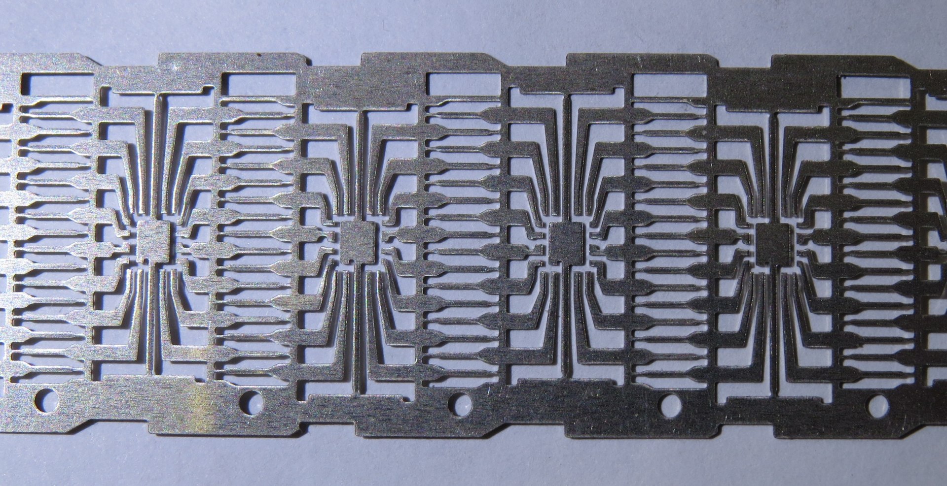
Field serviceability was also a selling point mentioned in the marketing literature. That feature no doubt came as a result of what was probably the overriding design goal: cheap, rapid manufacturing methods. Inside the DIP package, the IC die itself is mounted to a metal assembly called the lead frame. The lead frame is easily formed by a progressive stamping press, in which a series of dies punch the part out of a continuous coil of sheet metal stock. The lead frames can be stamped, the dies affixed, the die pads bonded to the leads by ultrafine wires, and the assembly encapsulated in one continuous process. Folding the leads down perpendicular to the device’s body is the final step, and leaves the leads exposed at the top of the chip, allowing access to testing instruments.
Following these design goals, devices in the dual in-line package started hitting the market in 1965. Fairchild originally concentrated on ceramic encapsulation, in an attempt to provide the same hermetic seal specified by the military for their devices. Later, encapsulation in plastic resin was introduced for less stringent environmental regimes, which drove the unit cost down drastically.
As a result of great design, low cost, and support for increasingly complex dies, the DIP was a wildly successful package for most of 50 years. Its basic design was extended to support more leads and larger dies, but eventually, technology surpassed the venerable design, and by the late 2000s some new chips were no longer available packaged in DIPs. The PCB world may be ruled by surface mount devices now, but that would not be the case if the design of Forbes, Rice, and Rogers hadn’t paved the way.


The flatpak was ahead of it’s time, since there was no way to automate soldering and the lead pitch was considered too small for easy hand work.
Anyone else remember the staggered sockets that Heathkit used so people didn’t have to contend with soldering 0.1 inch pitch parts? Now, imaging their reaction to the flatpak!
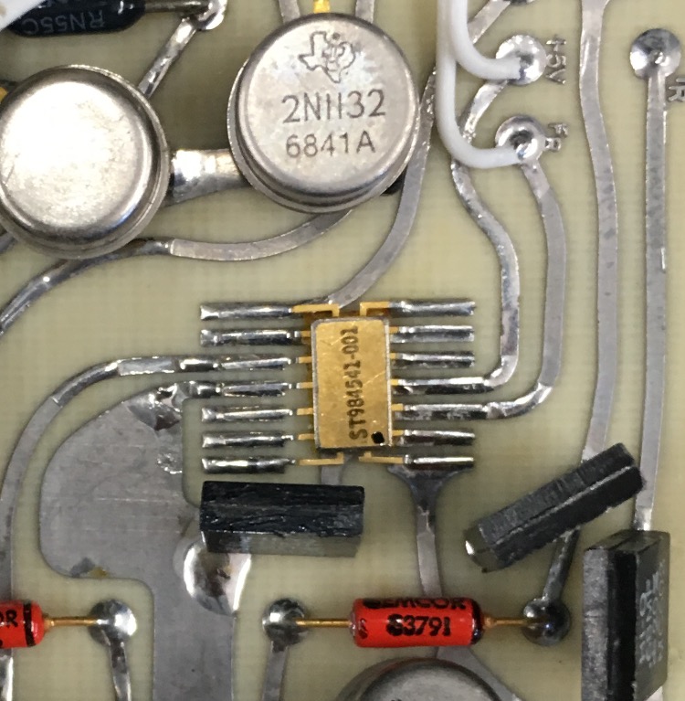
Another interesting artifact, if you will, is the positioning of the power supply pins at the upper right and lower left corners for some of the more common IC series, such as 54/7400 and 4000 series. Most of them are upper right/lower left, but a select few are not. (the 7490 comes to mind) One wonders why convention was broken for a few parts. There has to be a good back room story there…
I can only speculate the reasoning from what I know of high speed circuits.
The power and ground pin at the far end corners aren’t good design for high speed circuits as that arrangement have the highest lead inductances that can cause ground bounces i.e. overshoots and undershoots. See the lead frame picture above in the OP. Those pins are the *longest*. See the lead frame picture above in the OP where you have the shortest leads.
The ground reference internal to the chip is in series with the lead inductance and these bounces can alter what the input sees. As a counter, multiple pins could be switching at the same time during counter further compounding the effects. Glitches can affect the stored count values vs the transient nature in a combinational circuit.
Furthermore, these leads are close to the counter output reducing the loop area of the forward/return current flow. New (fast) wide fanout chips these days have interleaving power/ground pins breaking up groups of outputs.
In the ’80s, when DIP was king, one of the chip companies released a line with the power pins in the middle and felt the need to explain the decision as well as give a bit of history. Basically, some of the early chips had the power pins in the middle for exactly the reason you state. Design improvements made it possible to move the pins to the corners during the time most of the 74xx line was developed, and then speeds and output drive increased, forcing changes.
When doing layout, it’s convenient to have power & ground next to each other. I mean, you’re going to have a 0.1 uF cap across the lines anyway…
OTOH, if there are legit inside-the-package reasons for the pinout, I won’t complain.
Often the decoupling caps were soldered diagonally across the top of the chip—it looked a little bit like an afterthought, I’ve seen special purpose DIP sockets with the decoupling cap permanently installed on the 7-14 pair, too.
Finally, the PCB layout sometimes was simplified for a pipeline-type circuits, when the inputs were primarily on pins 1-6 and outputs on pins 8-13; the chips were placed parallel to each other, inter-chip signal connections ran between the chips, and power and ground buses were running in between the rows of the chips, with stubs to 7 and 14, like in
https://i.stack.imgur.com/KROrT.jpg
I think this is probably the answer. It’s certainly easier to lay out your power when you can feed a whole row of chips without any vias or jumpers, etc.
Also, I’m pretty sure single sided boards were a lot more common back then than they are today. If you had to wire jump anytime you need to cross over a trace, the simplicity in layout would be worth it.
Since most signal and switching speeds were also very slow by today’s standards, the tradeoffs in trace inductance and such were probably not the biggest concern.
The 7475 quad latch is another odd one, often used with the 7490, but not the same pinout. I did use to wonder. Maybe the series wasn’t designed in order, so they came before standardized pinouts? I don’t see a pattern that suggests the pins were chosen for the devices to line up better. Memory says that after some of those early strays, later additions kept to the “standard”.
Michael
The 7400 series was definitely not numbered chronologically.
There were a few (if I recall correctly) where the flatpack pinout differed from the dual inline pinout. There was at least one where the low power TTL (74Lxx) pinout differed from the standard TTL (74xx) pinout.
Flatpack leads were rather fragile; careless handling could destroy a device and desoldering was always an iffy proposition.
The first chips were allocated numbers in increments of 10: 5401, 5420 ,5430, etc. Later designs were numbered in between, generally following on from related chips.
As an example the original SN5470 was a J-K flip flop with AND gates in the inputs. Subsequent flip-flops were numbered ’71, ’72, etc, including the one we remember today: the SN5474 / SN7474 dual D-type flip-flop.
Some of the early logic families and packaging used pins 4 & 11 for power.
I’ve actually seen someone cut a 74LS73 in half, just past the power pins, to get a single J-K flip-flop in a 10-pin DIP.
I looked into this myself some months ago.
The explanation is that those oddballs are hangovers from the precursors to the 7400 series.
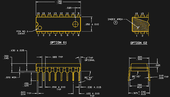
Before the series 54 and series 74 (as they were first known by TI) TTL chips, there were the series 51 RCTL and series 53 / 73 DTL logic chips. These were made in the ceramic flatpack package pictured above, and had power supply pins partway along each side (generally pins 3 and 7 for 10-pin Series 51, 3 and 8 for Series 53). There’s a 1965 databook showing pinouts for these at https://archive.org/details/bitsavers_tidataBookmiconductorIntegratedCircuitsJan65_14257211 . The pin count increased for the series 54 TTL chips (14 pins), but the power supply pins stayed in the midway position for all the flatpack packages (modern suffixes -W and -T).
For the 7400 series, all chips were provided in DIL packages instead. Whatever the reason, it seems to have been a policy decision to move the power supply pins to the corners at this point. I suspect this may have been done in anticipation of chips growing larger than 14 pins, and the desire to put the power pins in a consistent location.
TI’s TTL data books for the 1970s continue to list the old pinouts for the original SN54 series (such as the 5400, 5410, 5420, etc) alongside the new ones, but the newer 54S and 54LS come in the new corner-power layout, even in flatpack packages. Later additions to the family, such as the ’08 and ’32, were only ever manufactured in the new corner-power layout, even for the original SN54 series in flatpack packages. Conversely, some niche designs, such as the ’81 “16-bit RAM” and the ’90 “decade counter” kept the halfway-power layout even for the DIL-based 7400 series, presumably because volume was so low it wasn’t worth redesigning the silicon
Nice graphic Joe Kim!
+1, I would buy a poster of this
Me 3. Cover of the next omnibus?
Yeah, right?
He nailed it again, didn’t he? That’s an idea that Mike Szczys came up with, and Joe ran with it.
Absolutely would buy a poster.
I love these graphics the artist rocks it
+1
RIP DIP
Whenever people start talking about DIPs and chips I just want some guacamole.
There should be also mentioned problem with imperial vs metric systems and 2.5mm lead spacing in european chips. It was similar enough to 0.1 inch to use interchangably 16-pin ICs but not for 40-pin.
Heard stories about metric vs imperial pin pitch issues with Russian copies of western chips.
Funny that everybody switches to metric for new parts these days. :P
It is interesting to note the ways they were trying to keep the leads apart (https://www.langrex.co.uk/products/mc1709cglm709ch-op-amp-motorola-metal-can-ic/) this shows the green FP8-800 (for 8 lead can) which attempted to keep the leads from touching each other.
Funny that you mention that! Someone’s grandfather at my FRC high school during high school bequeathed some of his components on me, and among them are at least 100 canned ICs, along with several of those lead straighteners. Fun stuff!
I remember that plenty of those cans had plastic spacer disks underneath them with holes for the leads, I always wondered why that was done.
“The history of the DIP is shrouded in mystery, which is somewhat unusual for an industry that trumpets innovations far and wide and routinely patents everything.”
No, it’s not that unusual. All industry and patents really tell you is who got to make money off an idea not whose idea it was. Practically all the BIG inventions are full of conflicting stories and controversy. Just ask Edwin Armstrong or Gustave Whitehead!
Still doesn’t explain why nobody seems to be able to find a patent that covers the original design.
Thing is, I know where the information is. I was in touch with the curators at the Computer History Museum, where they have the original lab notebooks from Fairchild. Don Forbes’ notebook is there, covering the time period during which he was working on the DIP. I would have loved to get my hands on those, but time ran out.
The CHM is an amazing resource. Just the Fairchild notebook collection is a treasure trove – notebooks from Gordon Moore and Andy Groves! Imagine browsing through those. And the people were incredibly helpful – I emailed them after hours on a Friday and they got back to me almost immediately.
So is the 64-pin DIP the biggest DIP? I remember seeing the original Mac motherboard and being impressed at how the 68K CPU was similar in size to an entire row of DRAM chips.
I was at a computer club meeting in Southern California in the ’70s when a rep came to talk about a new processor (TI?) that came in a 64 pin dip. He said they were giving one away, skate board wheels not included.
I want to know is why the DIP IC had a symmetrical package that could be inserted backwards. Prior to that, every electronic component I can think of had some form of keying to prevent that. The case or pins were always asymmetric, or designed in such a way that putting it in backwards made no difference.
Just as there were no standards for power and ground pins, there were also no standards for how pin 1 end is marked. On some ICs, it is impossible to tell without outside information.
I’ve worked at companies where entire production runs of PCBs had to be scrapped or reworked because ICs got inserted backward. Think about how many millions of $$$ must have been wasted by these sorts of mistakes.
Of course, once a bad idea gets started, it continues…
well, a TO92 can be inserted backwards, and will probably burn/not work; the DIP packages always have a marker near pin 1 (either a dot in the corner or a half-circle impression on the edge above pin 1.
Not everyone used the dot or the half circle unfortunately. Some use a square indentation, some only taper that side of the DIP (particularly on the new, SOIC type packages). There are a few others, mostly old, I’d have to look at my collection that is at home.
There are also some alternate pin layouts. 0.1 spacing by far the most common, but I have some older audio ICs in which the center 3 pins are a single wide pin used as a heatsink. Some are bent over, some splay out with holes to bolt it down. There are also some oddballs that have alternating pins on 0.2″ spacing. Odd pins are close to the body, even pins are 0.1″ further out.
There are several ‘standard’ and a couple of oddball widths and lengths too. Wasn’t until the 80’s that you saw more than 20 pins in a narrow DIP very often for example.
I have always found it easy to insert through-hole diodes and electrolytic capacitors backwards, if I’m not careful about the markings.
Many modern SMT ICs can be installed backwards, and I have no doubt that a staggering amount of money has been spent over the years fixing and avoiding problems with misoriented parts. Some asymmetry in the package design could be helpful.
Automated pick and place machines, multilayer boards and conventions help. It’s rare to see a board with different ICs mounted 180 degrees rotated from each other. You might find 90 degree rotations in some boards where space is at an absolute premium, but in general it’s easier to keep all chips oriented the same way and route appropriately. The chips come out of the reel identically oriented, and then the same orientation programming is used for the pick and place. It makes it easy on the programmer to begin with. After the first board assembled is tested, every board that follows will be the same. In the through-hole days there was a lot of manual placement, making it difficult to assemble every board identically, with SMT and automation it’s difficult to assemble one different from the others.
It’s definitely not _rare_ to find boards with chips in all orientations. There is a bias towards having them in the same direction, as most boards will have a signal flow generally in one direction, and most ICs have pinouts with a signal flow in one general direction. (for example, almost all of the 74 series have the gates inputs pointing towards pin 1)
There are plenty of components, though, where this isn’t the case (microcontrollers, etc), and those will be in whatever orientation made most sense to the person laying out the board.
The 7402 is a notable exception.
We do not have any rule stating that ICs should have the same orientation. We mostly try to have the layout for repeating blocks the same but with the automated SMD manufacturing and AOI the computers just use the data from the layout program. It males no difference, if pin 1 looks the same direction or not for neighboring chips.
The SMT parts comes in on tape and reel. The the holes for the sprocket feed is on one side only while the peel off tape is on top, so there isn’t anyway for the tape to be inserted backwards or both backwards and upside down. The pick & place is programmed from CAD data generated from the PCB layout tool with orientation and X,Y coordinate.
Unfortunately IRL I have seen 90 degrees for 5mmx7mm ceramic oscillator. The oscillator is rectangular and that doesn’t help the 90 degrees rotation. Also 180 degrees for Tantalum cap, Zener diode where in both cases causes smoke.
Nothing beats the mixup on electrolytic vs semiconductor capacitor markings.
Electron flow?
My favorite experience was with a design a colleague wanted fabricated. He did some simulations in some version of spice, and there was a ‘helpful’ layout tool which would allow you to push the design into pc layout.
I domt know what crackhead did the library on standard sized passives. The tantalums had a mark in silkscreen on the NEGATIVE pin of the capacitor. This was a circuit that did some high current regulation for a lipo bank, feeding some piece of unobtanium. Thermally conductive filled bias, massive thermal relief, etc.
The engineer wasn’t around, I populated by schematic and refdes. You can guess the rest. After some surprises and back and forth once I got hold of the engineer, it performed flawlessly, but man, talk about an object lesson in why you verify polarity.
Filled vias, not bias. Dann you, autocorrect!
When I worked for ICL in the late sixties we were just introducing LEDs to replace miniature incandescent bulbs. And we had enormous difficulty in persuading the assembly ladies that it mattered which way round they went. As far as the ladies were concerned they were lamps and lamps aren’t polarised. In the end we had LEDs made with three leads in a triangular layout. (and “lady” is a courtesy title that some of them didn’t deserve :-))
Next up; Do Fuses have a polarity… ever?
Backwards? I never met the tech, but after 4 hours of no courage to ask on his first day, how to tell where pin 1 was on an IC, he was quietly walked out. Backwards? I’ve never seen ANYthing that was not somehow, marked.
A few decades ago I was working on the design of a minor part of a satellite that used logic ICs that were equivalent to 54LS series TTL. The first run of the boards didn’t work, and I traced it to one of the ICs being inserted backwards (i.e. 180 degree rotated).
The pin 1 dot printed on the top of the package actually denoted pin 8. Yay.
When we complained to Hughes (who supplied the ICs), they pointed out that there was a bump on the lead frame that correctly indicated pin 1, as shown in the documentation. The bump was too small to see with the naked eye.
BTW I worked out that the IC was rotated w.r.t. its pin 1 dot by measuring each pin with a multimeter set to diode test.
I had an IC with the usual part number printed up side down with respect to the depression on the package. I think I decided to trust the package. That was a long time ago before all the laser engraving days.
I once got a bunch of prototypes where all BC846NP double transistors were fitted backwards. Somebody who rigged up the pick and place machine interpreted “bipolar” creatively as “rotationally symmetric”, which is true for BC648S (NN) and BC856S (PP), but not for the NPN/PNP combination. They manually reworked it.
A “hammer fuse” may not have “polarity”, but it does have orientation.
Sometimes very badly marked. I’ve gotten plenty of chips before which are marked with a dot for pin 1, as described in their datasheets, but have another (often bigger) dot on another corner. It Seems common on STM32, though the extra dots are only in some batches. Others are fine. To make things worse, most manufacturers have pin 1 in the upper left corner relative to the text (obviously this isn’t a rule, and you should never count on that), and ST has it in the lower left. Atmega2560 chips usually all have one small dot (in the expected upper left corner), and 2 big dots on opposite corners. It’s certainly not the most clear.
Some Cyclone chips also have that and you have to somehow guess.
DIP was first called DIL for Dual In-Line. There was also SIL. Single sided chips and later QIL – Quad In-Line.
The early IC’s were often 8 pin round and people would layout PCB traces as DIL and bent the pins to fit.
A lot of PCB work back then was single sided as PTH (vias) was far too expensive. Putting a round part into a DIL PCB footprint meant a lot more trace routing options. Keep in mind that PCBs were hand drawn then so traces were thick.
Perhaps the DIL footprint came before the DIL package as manufacturers saw how PCBs were being laid out.
Before the distinction was lost, DIP stood for Dual Inline Plastic.
So now you’re going to tell us what they called the dual-inline ceramic package, right?
DIC! Lol
Where’s the article all I see is a picture?
Welcome to Web 3.0, the Internet for the illiterati
Our hosting service pushed an update that broke our page (and everyone else’s they host) for about 20 minutes on Thursday. Should all be back to normal now.
It looks like HaD abruptly changed the format for its blog page, so that we see only headlines there. Unfortunately, the link to the article also shows only the headline. Where is the actual article?
Heh…. It’s really funny to watch nowaday’s so-called experts tell all about the dip design and chips that I was so much drooling over and fending off the wife’s budget concerns due to cost per piece back in the day. Yes, it was truly increadible when I keyed in the first machine language pgm over a hour’s time via 8 dip switches and an input pb then switched it to “run” and BY GOSH the LED started to blink once a second as intended! It was so gratifying! It counted the seconds accurately, but it was only a few blinks before the broom whacked me upside the head as she yelled… “You spent HOW MUCH to make a light blink?!!”
Our hosts are missing the point of hacking. It’s not hacking, it’s learning. And I applaud anyone hacking. These commentators and self-appointed judges… well… I ducked the broom, and you should discount these “judges”.
Just hack on! I invite you with the greatest enthusiasm. You’ll have a blast, just use earplugs to remove all these supposed experts. Do what you like, as long as you like what you do.
I remember the first DIP I ever saw back in 1967. A friend had brought it home from his part time job and we sat in the pub marvelling that “There are over thirty transistors in that little package!!”
I think the first DIP I saw was analog – an op amp. They started appearing in electronic magazine articles in the very late 60s; I think the first decent project I worked on with op-amps was a synth project at school. That must have been about 1973.
And the pins were numbered the same way as vacuum tubes, a.k.a. Hollow State devices: looking at the solder side, notch or index at the bottom, pin 1 is on the left, numbers increase clockwise.
You aren’t a true electronics freak unless you have stepped on a DIP IC barefoot, laying upside down in your bedroom and had the pins stick into you. Leaving a twin line of dots in your skin. Oh yeah….
At the time I worked with electronics in my bedroom (school kid) the chips were way to precious (expensive, at least in relation to my pocket money) to leave them carelessly lying around on the floor.
Here’s a DIL chip, TBA540Q (date code 7442) which has had alternate leads bent in and out to increase the spacing and make the PCB layout easier: https://www.flickr.com/photos/anachrocomputer/26503283836
Quite a common thing to see in old colour TV circuits: https://www.flickr.com/photos/anachrocomputer/26436907772