These days we’ve got powerful free tools to do CAD and circuit design, cheap desktop 3D printers that can knock out bespoke enclosures, and convenient services that will spin up a stack of your PCBs and send them hurtling towards your front door for far less than anyone could have imagined. In short, if you want to build your own professional-looking gadgets, the only limit is your time and ambition. Well, assuming you only want to build a few of them, anyway.
Once you start adding some zeros to the number of units you’re looking to produce, hand assembling PCBs quickly becomes a non-starter. Enter the pick and place machine. This wonder of modern technology can drop all those microscopic components on your board in a fraction of the time it would take a human, and never needs to take a bathroom break. This week Chris Denney stopped by the Hack Chat to talk about these incredible machines and all the minutiae of turning your circuit board design into a finished product.
 Chris is the Chief Technology Officer (CTO) of Worthington Assembly, a quick turn electronics manufacturer in South Deerfield, Massachusetts that has been building and shipping custom circuit boards since 1974. He knows a thing or two about PCB production, and looking to help junior and mid-level engineers create easier to manufacture designs, he started the “Pick, Place, Podcast” when COVID hit and in-person tours of the facility were no longer possible. Now he says he can tell when a board comes from a regular listener by how many of his tips make it into the design.
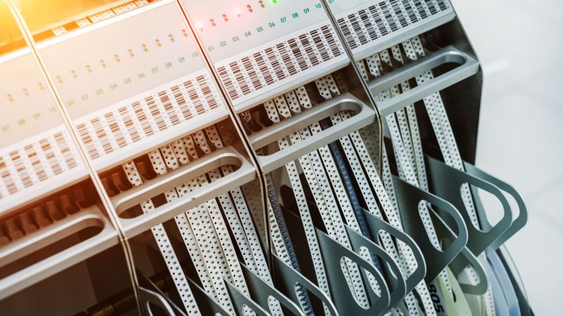
So what should you be doing to make sure your board assembly goes as smoothly as possible? Chris says a lot of it is pretty common sense stuff, like including clear polarity indicators, having a legible silkscreen, and the use of fiducial markers. But some of the tips might come as something of a surprise, such as his advice to stick with the classic green solder mask. While modern board houses might let you select from a rainbow of colors, the fact is that green is what most equipment has been historically designed to work with.
That black PCB might look slick, but can confuse older pick and place machines or conveyors which were designed with the reflectivity of the classic green PCB in mind. It also makes automated optical inspection (AOI) much more difficult, especially with smaller component packages. That said, other colors such as white and red are less of a problem and often just require some fine tuning of the equipment.
He also pulled back the curtain a bit on how the contract manufacturing (CM) world works. While many might have the impression that the PCB game has moved overseas, Chris says orders of less than 10,000 units are still largely handheld by domestic CMs to minimize turnaround time. He also notes that many assembly houses are supported almost entirely by a few key accounts, so while they may be juggling 50 customers, there’s usually just two or three “big fish” that provide 80% of their business. With such a tight-knit group, he cautions CMs can be a bit selective; so if a customer is difficult to work with they can easily find themselves on the short end of the stick.
While the Hack Chat is officially only scheduled for an hour, Chris hung out for closer to three, chatting with community members about everything and anything to do with electronic design and production. His knowledge and passion for the subject was readily apparent, and we’re glad he was able to make time in his schedule to join us.
The Hack Chat is a weekly online chat session hosted by leading experts from all corners of the hardware hacking universe. It’s a great way for hackers connect in a fun and informal way, but if you can’t make it live, these overview posts as well as the transcripts posted to Hackaday.io make sure you don’t miss out.


Two things noted that deserve expanding on: Humans are slow, yes, and the game is local and not overseas, yes as well. The reason is that human labour is much cheaper than pnp, performances and time are worse, but to get boards assembled on a budget, no one can beat the slave-like prices of overseas labour.
Your comment is about 20 or even 30years out of date. Offshore assembly houses have grown to a scale that alone gives them a competitive advantage, and they also have access to far more manufacturing engineering talent than is available in the U.S. I was the operations manager for a large U.S. semiconductor manufacturer, and we did a lot of our manufacturing offshore for several reasons that went well beyond labor cost. Things like better access to Asian markets, lower operating overhead, cooperative governments (we put a wafer fab offshore purely because the local city officials told us it would take 18 months for approvals even though we agreed to all their conditions in advance), better access to raw materials, etc. Chinese universities turn out manufacturing engineers by the thousands … young people in the U.S. are mostly not interested in those curricula. Most Chinese pick&place operations are HEAVILY automated.
I suspect that a couple of 3D printers could be modified to perform a small scale pick&place operation for single sided boards. Modify one one printer to extrude solder paste, and replace the extruder on the second printer with a vacuum tip. The small lengths of tapes for the components could be pinned off to the side of a modified heat bed. It would take some software changes of course.
OpenPNP is more polished I suspect. I hear the project has evolved nicely.
This matte black solder mask which has become fashionable of late makes it very hard to see the tracks, unlike the usual green, or even red, yellow , blue masks. Purple mask looks great. The matte black mask has become the blue LED of pcbs
Why would you need to see the tracks though? I worked in assembly for year and the only time you needed to know where a track was located, was for modifications such as cutting a trace or adding a modification wire.
If it’s really required all you need to do is print out the gerber or sand the resist off a spare copy of the PCB.
True, from a production point of view, you may not need to see the tracks. My comment is more from a hobbyist/developer view, and also my own disagreement with the “black mask is cool” thing. To each his own
I’ve seen worse: a fab decided that silkscreen was not needed and they ordered black pcb’s. In the production run for 250 pieces the swapped the orientation on all placed optos ( eight per board)
Needless to say the had a very bad week.
So yes. You need silkscreen an yes you need visible tracks. Just to make shure there are made no interpretation mistakes.
We don’t make shure, unless we are making microphones…