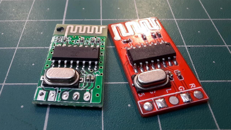
There was a time when we would start our electronic projects with integrated circuits and other components, mounted on stripboard, or maybe on a custom PCB. This is still the case for many devices, but it has become increasingly common for an inexpensive ready-built module to be treated as a component where once it would have been a project in its own right. We’re pleased then to see the work of [ElectroBoy], who has combined something of both approaches by reverse engineering the pinout of a Chinese Bluetooth audio chip with minimal datasheet, and making his own take on an off-the-shelf Bluetooth audio module.
The JL_AC6939B comes in an SOIC16 package and requires a minimum number of components. The PCB is therefore a relatively simple proposition and indeed he’s fitted all parts and traces on one side with the other being a copper ground plane. It’s dangerous to assume that’s all there is to a board like this one though, because many an engineer has come unstuck trying to design a PCB antenna. We’d hazard a guess that the antenna here is simply a wavy PCB line rather than an antenna with a known impedance and bandwidth, at the very least it looks to have much thicker traces than the one it’s copying.
It’s possible that it’s not really worth the effort of making a module that can be bought for relative pennies ready-made, but to dismiss it is to miss the point. We make things because we can, and not merely because we should.


From what I’ve read in the past these JL chips (at least some of them) are full-blown microcontrollers that can be programmed to do a ton of stuff. Some can do FM radio and bluetooth in the same package as well. I really wish these were better documented, they could be very cool for a ton of DIY projects.
Yes they are a really functional chip. One programmed version is KT1025A / BT201 that gives both audio and serial port.
Some work on programming them here: https://github.com/christian-kramer/JieLi-AC690X-Familiarization
This wasn’t done “because we can” but because it’s an advert for JLCPCB. Getting a bit sick of this kind of “project” appearing everywhere.
And with that, I really doubt this fail of imitating the antenna.
There are a lot of parameters that together need to match the frequency. Such a solder blob on top surely doesn’t help.
There is a reason why those inverted F antenna do not have solder mask on. That’s might seem to be a small thing, but the solder mask acts as a dielectric and it can detune the antenna.
Now someone actually put in solder on top of the traces. The thickness of solder is uncontrolled, so good luck reproducing it. I would think copper has better conductivity than solder. Skin depth at high frequency means that you’ll have signals going in the solder thus a higher loss.
That is if the whole antenna was tuned for the 2.45GHz band in the first place.
It looks like someone have no idea what they are doing. If in doubt, measure and copy the whole layout exactly. i.e. desolder the board, scan it and import the bitmap to your layout program etc. Don’t make stuff up on your own.
Yet another useless .io writeup that contain no way for someone to learn how to do it or how to improve it.
It is an advert for a PCB manufacturer.
There are some really interesting projects on .io but sadly the signal-to-noise ratio is quite bad because there also are a LOT of (more or less explicit) adverts and other nonsense like free-energy-stuff and so on.
Wow yeah this is a rather blatant advert.
Basically all of [ElectroBoy]’s projects are, if I’m not mistaken.
Another solution https://fccid.io/2AEW6-TE1011/Schematics/Schematics-4402153.check.
The author of this .io has never heared anything about RF. Learning from it is learning to fail. The chinese module one looks like someone has cared about impedance and so, don’t know if he has done it good, but someone cared about it. The other module looks like a uninformed reproduction of the schematic.
Suppose it will work, but with a worse signal-/noise ratio and more disturbance.
>at the very least it looks to have much thicker traces than the one it’s copying.
Meandered antennas are not strip lines, there is no ground plane below it either, so just the thickness is not something to look at and judge.
What matters more is that the footprints for the matching network have been omitted. Without these, it’s impossible to compensate deviations from the designed antenna to one made with a real-world PCB type and mounted in a detuning environment.
Workflow usually is: pick design, simulate and parameterize, build, measure, calculate compensation network, implement network and verify.
This video explains how: https://youtu.be/recnhI5Uj7w
It’s the “simulate” part of the above that costs $$$$$, He would most likely have gotten very close by copying the antenna trace from the manufactured board as closely as possible.
Some manufacturers provide full reference designs already, so test PCBs with a set of slightly varied antennas should get one there without simulation. E.g. “AN1088: Designing with an Inverted-F
2.4 GHz PCB Antenna”
Various tools such as NEC2 are free to use, as is smith chart software for the matching network.
I note he has missed out the Gnd stitching vias.
Or just use a chip antenna. For low volume or personal project, can’t beat having a simple part that has be tuned for the frequency and take up very little space. I would be very surprised that a place that carries the main chip won’t have the chip antenna.
There are also antenna with coax breakouts and all kinds of things like that from China.
I hate to hate on someone’s learning project, but they really shouldn’t be messing with RF if they don’t know what they’re doing.
Their antenna is all wrong, but there’s also ground inside the loops of the antenna and on the other side of the PCB! At best, this thing is gonna have crap range.
All of us started somewhere….
Agreed, learning is great–but the same way that you need a license to learn to drive a car, you also need a license to transmit on the radio spectrum we all share.
Not much harm in this particular case, but doing this sort of thing without a license or at least a basic understanding of radio should be discouraged.
May be learning by *reading* app. notes of similar parts. Too lazy to read is not a good excuse. There are tons of PCB antenna design articles by different vendors out there. Even a lazy google of “2.45GHz PCB antenna” would point you to the right direction.
RF stuff is a bit tricky as your PCB *IS* a component, so you’ll need to know the parameter by your particular PCB manufacturer.
2.45GHz chip antenna is a thing if you don’t want to go through the design/test process. They have done most of the tricky RF design stuff and you can get predictable result. The datasheet is only 4 pages long.
Saw that, too.
>they really shouldn’t be messing with RF if they don’t know what they’re doing.
Not seeing anything wrong with that (I mean what’s the harm?).
Putting it out there however – and worse, having it covered by Hackaday in a non-critical fashion- is where it gets disappointing.
>”It’s possible that it’s not really worth the effort”
The same could be said about reading this hackaday article. I’m sure there are a lot more projects out there on .io that are more deserving of constructive criticism from the audience than this zero-foxes board design and a “can’t share the BOM officially as per their rules” – value.
Looking at [ElectroBoy]’s other “projects”, I hazard a guess that we won’t be seeing a VNA connected to the antenna structure and an iterative process that shows a learning process, and instead just get yet another JLCPCB ad.
There was a time when we started our projects with transistors, resistors, inductors and capacitors…
There was a time when we took apart old tube radios to start projects.
A 5Ghz VNA now costs $250. So, maybe :-)
NEC2 simulation probably won’t help much. There may be free simulators out there that will, but the ones I know about are $multi-K. For that price you get ease of use and example setups. When I did a Bluetooth PCB antenna design, the chip manufacturer took our PCB layout file and ran it through their simulator, then sent me a markup telling me what to change. All for free (but we did end up buying a lot of their chips).
Good tip. Wherever possible, use the manufacturer. App notes are usually a good starting place. I say, “usually”, because I have found app notes with errors in them, The manufacturer rarely builds and tests their application circuits (Linear Tech, now part of Analog Devices is a notable exception) and some app notes are cut-and-paste from older app notes…you get the idea. But still, if you have no idea what to do, building the circuit (and using the PCB layout if possible) is probably your best starting point. Alternatively, buying a product with the part in it and stealing whatever you need from it — assuming the manufacturer got it right!
Some vendors have application engineers write their app. notes. It is funny to see the differences of recommendations from the datasheets vs the app. notes. The app. notes you want for RF and other tricky stuff is the one that comes with their evaluation board. Likely it would have been used by their development team at some point.
One of our smaller vendors solicited me to write one at one point, but I turned them down. :P
I really need a “dislike” button.
I don’t really see the “reverse engineering” part on this ¿project?
It’s more like a bad clone lf the ¿original? board.
I reslly don’t see any value on this ¿project?.
There’s one thing that is worse than having no starting point, and that’s having available material that sets one up for failure and ignorance, as is the case here.
I see value in having proven design macros, but is is not it.
Putting an unterminated meander line over a grounplane gives you a sucky antenna. The cheapest way of determining its suckiness is to compare the signal from a non-sucky antenna using a phone app at some distance away. I suppose it will radiate something when you are very close, as in the photos. If you want it to radiate less (you know, to reduce the 5G COVID radiation), put more vias around the delay line, tune the impedance by making it the proper width, and terminate the end with a resistor. But if you want to actually have an antenna, cut the ground plane off the underside and let it breathe RF. Also, don’t put solder pads right where you feed it.
So,… has anyone ever used these SDK’s by JL? does anyone know if it also covers those tiny QFN20 JL chips in my bluetooth earbuds? How hard would it be to reprogram the uC on these low cost consumer bluetooth products?
https://github.com/Jieli-Tech