With the never ending march of technological progress, arguably the most complex technologies become so close to magic as to be impenetrable to those outside the industry in which they operate. We’ve seen walkthrough video snapshots of just a small part of the operation of modern semiconductor fabs, but let’s face it, everything you see is pretty guarded, hidden away inside large sealed boxes for environmental control reasons, among others, and it’s hard to really see what’s going on inside.
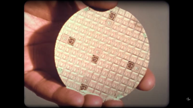
Let’s step back in time a few decades to 1983, with an interesting tour of the IC manufacturing facility at Bell Labs at Murray Hill (video, embedded below) and you can get a bit more of an idea of how the process works, albeit at a time when chips hosted mere tens of thousands of active devices, compared with the countless billions of today. This fab operates on three inch wafers, producing about 100 die each, with every one handled and processed by hand whereas modern wafers are much bigger, die often much smaller with the total die per wafer in the thousands and are never handled by a filthy human.
Particle counts of 100 per cubic foot might seem laughable by modern standards, but device geometries back then were comparatively large and the defect rate due to it was not so serious. We did chuckle somewhat seeing the operator staff all climb into their protective over suits, but open-faced with beards-a-plenty poking out into the breeze. Quite simply, full-on bunny suits were simply not necessary. Anyway, whilst the over suits were mostly for the environment, we did spot the occasional shot of an operator wearing some proper protective face shielding when performing some of the higher risk tasks, such as wafer cleaning, after all as the narrator says “these acids are strong enough to eat through the skin” and that would certainly ruin your afternoon.
No story about integrated circuit processing would be complete without mentioning the progress of [Sam Zeloof] and his DIY approach to making chips, and whilst he’s only managing device counts in the hundreds, this can only improve given time.


They made bigger chips too. A friend at Bell Labs and I developed an analog image sensor / neural net chip that was fabricated there in the late 80s. It was about 75mm square. Qty: 4. Boeing had similar in house capabilities.
Hey wouldn’t it be cool if we still did that instead of the whole world relying on Taiwan for some reason
You must have missed a few dozens of episodes of Asianometry…
“Particle counts of 100 per cubic foot might seem laughable by modern standards”
That’s comparable to ISO5, which is still really good! Modern standards for cleanrooms with people in them normally start at ISO5 and go up from there.
I’ve worked with 3 inch wafers in the early nineties in a class 10000 cleanroom; only in certain spots under certain benches class 100 could be achieved in that cleanroom.
@TG (sorry, I gave up on message threading)
This would only work if we stopped being cheapskates all over the place and kept reaching for the lowest price.
As it is, “we” have to find people “willing” to work for us for a fraction of a dollar an hour. Even if it takes a war or two.
In 1973, I took a “semiconductor design” course taught by a guy that worked at the local KC area Western Electric (WE) semi plant, but in the summers, he “moonlighted” at HP Labs where he “really had fun”. While we did cover some IC design stuff, like doping profiles (complementary error function etc.) and ionization processes, it was less taxing than trying to really make something. The instructor recounted “the days when” WE production of glass axial switching diodes used in phone systems then had a “keep” rate of about 5-15% which they thought was good. Back in the early days, they also had to worry about connections and packaging of semiconductors in order to get good, final product. I think we even had some mimeographed class handouts with the HP logo. He was not able to do what he wanted for a class project, namely gain access to the WE fab, so our final assignment wasn’t a semiconductor design, but a logic design: build a 4 bit TTL ALU that wasn’t a 74181 (I forget the exact nuance), but it was fun nonetheless, and challenging back then.
Is that really 1983? Looks more like mid-1970s to me.
and what reference made you draw that conclusion?
3 inch wafers, degraded 16mm film and the picture of the girl with a colorful dress in the film leader.
Forgot to mention the rather large chips with coarse structures. Could be a 6µm process like the one used for the 8080.
Did this from 1967 to1990. Started with 1.5″ diameter wafers.
I remember 1980 Motorola cmos plant we were fuming gold instead of aluminum… 6.5 hour shifts overnight grinding wafers on what looked like a giant lathe stone
I think an xref to https://hackaday.com/2022/02/08/hair-today-gone-tomorrow-four-men-go-to-fix-a-wafer-prober/ is in order, although by then they were using 200mm wafers (roughly 8″ rather than 3″).