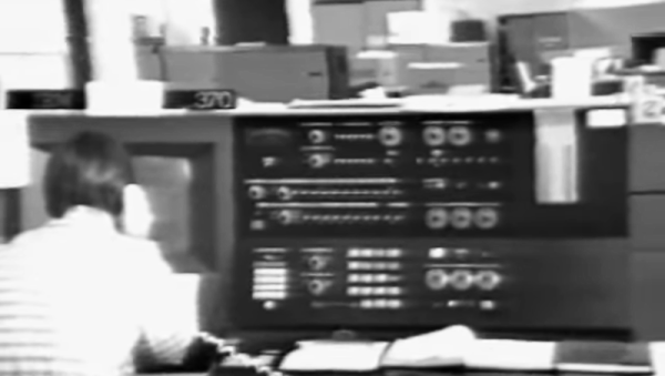
The Bellmac-32 CPU — What?

If you have never heard of the Bellmac-32, you aren’t alone. But it is a good bet that most, if not all, of the CPUs in your devices today use technology pioneered by this early 32-bit CPU. The chip was honored with the IEEE Milestone award, and [Willie Jones] explains why in a recent post in Spectrum.

The chip dates from the late 1970s. AT&T’s Bell Labs had a virtual monopoly on phones in the United States, but that was changing, and the government was pressing for divestiture. However, regulators finally allowed Bell to enter the computing market. There was only one problem: everyone else had a huge head start.

There was only one thing to do. There was no point in trying to catch the leaders. Bell decided to leap ahead of the pack. In a time when 8-bit processors were the norm and there were nascent 16-bit processors, they produced a 32-bit processor that ran at a — for the time — snappy 2 MHz.

Continue reading “The Bellmac-32 CPU — What?”

What Would It Take To Recreate Bell Labs?

It’s been said that the best way to stifle creativity by researchers is to demand that they produce immediately marketable technologies and products. This is also effectively the story of Bell Labs, originally founded as Bell Telephone Laboratories, Inc. in January 1925. As an integral part of AT&T and Western Electric, it enjoyed immense funding and owing to the stable financial situation of AT&T very little pressure to produce results. This led to the development of a wide range of technologies like the transistor, laser, photovoltaic cell, charge-coupled cell (CCD), Unix operating system and so on. After the break-up of AT&T, however, funding dried up and with it the discoveries that had once made Bell Labs such a famous entity. Which raises the question of what it would take to create a new Bell Labs?

As described in the article by [Brian Potter], one aspect of Bell Labs that made it so successful was that the researchers employed there could easily spend a few years tinkering on something that tickled their fancy, whether in the field of semiconductors, optics, metallurgy or something else entirely. There was some pressure to keep research focused on topics that might benefit the larger company, but that was about it, as the leadership knew that sometimes new technologies can take a few years or decades to come to fruition.

Continue reading “What Would It Take To Recreate Bell Labs?”

Bell Labs Is Leaving The Building

If you ever had the occasion to visit Bell Labs at Murray Hill, New Jersey, or any of the nearby satellite sites, but you didn’t work there, you were probably envious. For one thing, some of the most brilliant people in the world worked there. Plus, there is the weight of history — Bell Labs had a hand in ten Nobel prizes, five Turing awards, 22 IEEE Medals of Honor, and over 20,000 patents, including several that have literally changed the world. They developed, among other things, the transistor, Unix, and a host of other high-tech inventions. Of course, Bell Labs hasn’t been Bell for a while — Nokia now owns it. And Nokia has plans to move the headquarters lab from its historic Murray Hill campus to nearby New Brunswick. (That’s New Jersey, not Canada.)

If your friends aren’t impressed by Nobels, it is worth mentioning the lab has also won five Emmy awards, a Grammy, and an Academy award. Not bad for a bunch of engineers and scientists. Nokia bought Alcatel-Lucent, who had wound up with Bell Labs after the phone company was split up and AT&T spun off Lucent.

Continue reading “Bell Labs Is Leaving The Building”

Retrotechtacular: The Computer Center Of 1973

You might expect Bell Labs would have state-of-the-art computers, and they did. But it is jarring to realize just how little that was in 1973, fifty years ago. If you started work at Bell’s Holmdel Computing Center back then, you might have watched one of the orientation videos below. Your first clue about how far things have come might be the reference to the IBM 370/165, which had “3 million bytes of core, 2 million of which are available for programmer use.” Even our laptops today have at least 8 gigabytes of RAM. There were at least two other smaller IBM 370s, too. Plenty of 029 card punches are visible.

If you were trying to run something between 8:00 AM and 5:30 PM, you had to limit your job run time to three minutes, 4,000 lines of output, and no more than 1,000 cards in and 5,000 cards out. Oh, and don’t use more than 384 kB of that core memory, either. If you fell within those limits, you could hand your card deck over at the express counter and get your results in only five or ten minutes. If you were not in the express line but still rated “premium” service, you could expect to wait a half hour.

Continue reading “Retrotechtacular: The Computer Center Of 1973”

Hackaday Links Column Banner

Hackaday Links: December 11, 2022

“They paved paradise and put up a parking lot.” That might be stretching things a bit, especially when the “paradise” in question is in New Jersey, but there’s a move afoot to redevelop the site of the original “Big Bang Antenna” that has some people pretty upset. Known simply as “The Horn Antenna” since it was built by Bell Labs in 1959 atop a hill in Holmdel, New Jersey, the antenna was originally designed to study long-distance microwave communications. But in 1964, Bell Labs researchers Arno Penzias and Robert Wilson accidentally discovered the microwave remnants of the Big Bang, the cosmic background radiation, using the antenna, earning it a place in scientific history. So far, the only action taken by the township committee has been to authorize a study to look into whether the site should be redeveloped. But the fact that the site is one of the highest points in Monmouth County with sweeping views of Manhattan has some people wondering what’s really on tap for the site. A petition to save the antenna currently has about 3,400 signatures, so you might want to check that out — after all, you don’t know what you’ve got ’til it’s gone.

Continue reading “Hackaday Links: December 11, 2022”

Integrated Circuit Manufacturing At Bell Labs In 1983

With the never ending march of technological progress, arguably the most complex technologies become so close to magic as to be impenetrable to those outside the industry in which they operate. We’ve seen walkthrough video snapshots of just a small part of the operation of modern semiconductor fabs, but let’s face it, everything you see is pretty guarded, hidden away inside large sealed boxes for environmental control reasons, among others, and it’s hard to really see what’s going on inside.

Let’s step back in time a few decades to 1983, with an interesting tour of the IC manufacturing facility at Bell Labs at Murray Hill (video, embedded below) and you can get a bit more of an idea of how the process works, albeit at a time when chips hosted mere tens of thousands of active devices, compared with the countless billions of today. This fab operates on three inch wafers, producing about 100 die each, with every one handled and processed by hand whereas modern wafers are much bigger, die often much smaller with the total die per wafer in the thousands and are never handled by a filthy human.

Particle counts of 100 per cubic foot might seem laughable by modern standards, but device geometries back then were comparatively large and the defect rate due to it was not so serious. We did chuckle somewhat seeing the operator staff all climb into their protective over suits, but open-faced with beards-a-plenty poking out into the breeze. Quite simply, full-on bunny suits were simply not necessary. Anyway, whilst the over suits were mostly for the environment, we did spot the occasional shot of an operator wearing some proper protective face shielding when performing some of the higher risk tasks, such as wafer cleaning, after all as the narrator says “these acids are strong enough to eat through the skin” and that would certainly ruin your afternoon.

No story about integrated circuit processing would be complete without mentioning the progress of [Sam Zeloof] and his DIY approach to making chips, and whilst he’s only managing device counts in the hundreds, this can only improve given time.

Continue reading “Integrated Circuit Manufacturing At Bell Labs In 1983”

Retrotechtacular: The Forgotten Vacuum Tube A/D Converters Of 1965

In any era, the story of electronics has very much been about figuring out how to make something happen with what’s available at the time. And as is often the case, the most interesting developments come from occasions when needs exceed what’s available. That’s when real innovation takes place, even if circumstances conspire to keep the innovation from ever taking hold in the marketplace.

This gem of a video from the Antique Wireless Association has a perfect example of this: the long-lost analog-to-digital converter vacuum tube. Like almost every mid-20th-century innovation in electronics, this one traces its roots back to the Bell Laboratories, which was keenly interested in improving bandwidth on its massive network of copper lines and microwave links. As early as 1947, one Dr. Frank Gray, a physicist at Bell Labs, had been working on a vacuum tube that could directly convert an analog signal into a digital representation. His solution was a cathode ray tube similar to the CRT in an oscilloscope. A beam of electrons would shine down the length of the tube onto a shadow mask containing holes arranged in a “reflected binary code,” which would later be known as a Gray code. The analog signal to be digitized was applied to a pair of vertical deflector plates, which moved the beam into a position along the plate corresponding to the voltage. A pair of horizontal deflector plates would then scan the beam across the shadow mask; where electrons fell on a hole, they would pass through to an output plate to be registered as a bit to be set.

Continue reading “Retrotechtacular: The Forgotten Vacuum Tube A/D Converters Of 1965”