Integrated Circuit Manufacturing At Bell Labs In 1983

With the never ending march of technological progress, arguably the most complex technologies become so close to magic as to be impenetrable to those outside the industry in which they operate. We’ve seen walkthrough video snapshots of just a small part of the operation of modern semiconductor fabs, but let’s face it, everything you see is pretty guarded, hidden away inside large sealed boxes for environmental control reasons, among others, and it’s hard to really see what’s going on inside.

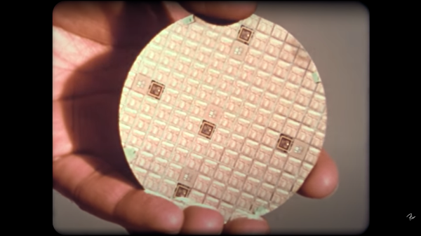
Let’s step back in time a few decades to 1983, with an interesting tour of the IC manufacturing facility at Bell Labs at Murray Hill (video, embedded below) and you can get a bit more of an idea of how the process works, albeit at a time when chips hosted mere tens of thousands of active devices, compared with the countless billions of today. This fab operates on three inch wafers, producing about 100 die each, with every one handled and processed by hand whereas modern wafers are much bigger, die often much smaller with the total die per wafer in the thousands and are never handled by a filthy human.

Particle counts of 100 per cubic foot might seem laughable by modern standards, but device geometries back then were comparatively large and the defect rate due to it was not so serious. We did chuckle somewhat seeing the operator staff all climb into their protective over suits, but open-faced with beards-a-plenty poking out into the breeze. Quite simply, full-on bunny suits were simply not necessary. Anyway, whilst the over suits were mostly for the environment, we did spot the occasional shot of an operator wearing some proper protective face shielding when performing some of the higher risk tasks, such as wafer cleaning, after all as the narrator says “these acids are strong enough to eat through the skin” and that would certainly ruin your afternoon.

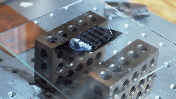
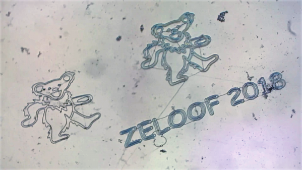
No story about integrated circuit processing would be complete without mentioning the progress of [Sam Zeloof] and his DIY approach to making chips, and whilst he’s only managing device counts in the hundreds, this can only improve given time.

Continue reading “Integrated Circuit Manufacturing At Bell Labs In 1983”

Laser doping silicon wafer

Laser Doping His Way To Homemade Silicon Chips

It’s a pity that more electronics enthusiasts haven’t taken the hobby to its ultimate level: making your own semiconductors. There are plenty of good reasons for that: chief among them is the huge expense involved in obtaining the necessary equipment. But for the sufficiently clever, there are ways around that.

[Zachary Tong] is dipping his toes into the DIY semiconductor world, and further to the goal of keeping costs to a hobbyist scale, is experimenting with laser doping of silicon. Doping is the process of adding impurities to silicon wafers in a controlled manner to alter the electrical properties of the semiconductor. [Zach]’s doping method is a more localized version of the simple thermal diffusion method, which drives a dopant like phosphorus into silicon using high temperatures, but instead of using a tube furnace, he’s using a fiber laser.

The video below shows his two-step process, which first blasts the silicon oxide layer off the wafer before doping with the laser shining through a bath of phosphoric acid. The process is admittedly fussy, and the results were mixed at best. [Zach]’s testing seems to suggest that some doping occurred, and it even looks like he managed to make something reasonably diode-like using the method.

Although the jury is still out on [Zach]’s method, we thought the effort was the important bit here. Granted, not everyone has a fiber laser kicking around to replicate his results, but it’s always good to see progress in the DIY semiconductor field. Here’s hoping [Zach]’s work, along with the stuff that [Sam Zeloof] is doing, kicks off a spate of garage semiconductor fabs.

Continue reading “Laser Doping His Way To Homemade Silicon Chips”

Tiny Art Etched Into Silicon Wafers With Electron Beam Lithography

Looks like [Sam Zeloof] got bored on his Thanksgiving break, and things got a little weird in his garage. Of course when your garage contains a scanning electron microscope, the definition of weird can include experimenting with electron-beam lithography, resulting in tiny images etched into silicon.

You’ll probably remember [Sam] from his 2018 Hackaday Superconference talk on his DIY semiconductor fab lab, which he used to create a real integrated circuit. That chip, a PMOS dual-channel differential amp, was produced by photolithography using a modified DLP projector. Photolithography imposes limits to how small a feature can be created on silicon, based on the wavelength of light.

[Sam] is now looking into using the electron beam of his SEM as a sort of CNC laser engraver to produce much finer features. The process involves spin-coating silicon wafers with SU-8, an epoxy photoresist normally used with UV light but that also turns out to be sensitive to electron beams. He had to modify his SEM to control the X- and Y-axis deflection with a 12-bit DAC and provide a custom beam blanker. With a coated wafer in the vacuum chamber, standard laser engraving software generates the G-code to trace his test images on the resist. A very quick dip in acetone develops the exposed chip.

[Sam] says these first test images are not too dainty; the bears are about 2.5 mm high, and the line width is about 10 μm. His system is currently capable of resolving down to 100 nm, while commercial electron beam lithography can get down to 5 nm or so. He says that adding a Faraday cage to the setup might help him get there. Sounds like a project for Christmas break.

Continue reading “Tiny Art Etched Into Silicon Wafers With Electron Beam Lithography”

Making Solar Cells

We will admit that it is unlikely you have enough gear in your basement to make a solar cell using these steps. However, it is interesting to see how a bare silicon wafer becomes a solar cell. If you’ve seen ICs going through fabrication, you’ll see a lot of similarities, but there are some differences.

The process calls for a silicon wafer, some ovens, spin coaters, photolithography equipment, and a dice saw, among other things. Oh, you probably also need a clean room. Maybe you should just buy your solar cells off the shelf, but it is still interesting to see how they are made.

Modern solar cells have some extra structures to improve their efficiency, but the cells in this video are pretty garden-variety. For example, some experimental cells use multiple layers of active devices, each tuned to absorb a different wavelength of light.

If you really want to make your own, there’s another process where you can start with some copper and wind up with a kind of solar cell that uses a copper-based semiconductor material. But don’t be fooled into thinking that making the silicon variety is totally out of reach to hackers, we’ve seen [Sam Zeloof] pull it off.

Continue reading “Making Solar Cells”

The Fab Lab Next Door: DIY Semiconductors

You think you’ve got it going on because you can wire up some eBay modules and make some LEDs blink, or because you designed your own PCB, or maybe even because you’re an RF wizard. Then you see that someone is fabricating semiconductors at home, and you realize there’s always another mountain to climb.

We were mesmerized when we first saw [Sam Zeloof]’s awesome garage-turned-semiconductor fab lab. He says he’s only been acquiring equipment since October of 2016, but in that short time he’s built quite an impressive array of gear; a spin-coating centrifuge, furnaces, tons of lab supplies and toxic chemicals, a turbomolecular vacuum pump, and a vacuum chamber that looks like something from a CERN lab.

[Sam]’s goal is to get set up for thin-film deposition so he can make integrated circuits, but with what he has on hand he’s managed to build a few diodes, some photovoltaic cells, and a couple of MOSFETs. He’s not growing silicon crystals and making his own wafers — yet — but relies on eBay to supply his wafers. The video below is a longish intro to [Sam]’s methods, and his YouTube channel has a video tour of his fab and a few videos on making specific devices.

[Sam] credits [Jeri Ellsworth]’s DIY semiconductor efforts, which we’ve covered before, as inspiration for his fab, and we’re going to be watching to see where he takes it from here. For now, though, we’d better boost the aspiration level of our future projects.

Continue reading “The Fab Lab Next Door: DIY Semiconductors”

Gas Containment For Laser Cutters

Tired of breathing all the noxious fumes your laser cutter puts out? Yeah… we don’t have a laser cutter either. But [Jeri Ellsworth] does and she needed a way to evacuate off-gases generated during cutting so that they don’t damage the laser cutter, or her lungs. What she came up with is a containment box that attaches to a pump system.

The problem is that you want to keep the gases away from the laser cutter hardware but you still need to be able to shoot the laser at your work material. Her clever solution is to use a silicone wafer like the ones with which she makes integrated circuits. They allow the infrared laser to pass through without being chopped in half. What you see in the image above is a red box with the round wafer in the center. Near the bottom of the image is a clear window so you can see what’s going on with your work piece. But to get the full idea you need to watch the video embedded after the break.

We can’t help but think she’s building this in preparation for some more chemistry hacking.

Continue reading “Gas Containment For Laser Cutters”

Transistor Fabrication: So Simple A Child Can Do It

If manufacturing printed circuit boards has become too easy you should try your hand at producing transistors. [Jeri Ellsworth] put together a collection of videos outlining the process. These go way beyond the IC fabrication we saw from her in the past. It doesn’t take much, a 1000 degree oven with steam option, silicone wafers, and a variety of chemicals. We’ve embedded the instructional video as well as two demonstrations of her N-style FET after the break. Continue reading “Transistor Fabrication: So Simple A Child Can Do It”