No matter how advanced your design skills, the chances are you’ll need to spend some time chasing bugs in your boards after they come back from the assembly house. Testing and debugging a PCB typically involves a lot of cross-checking between the board, the layout and the schematic, which quickly becomes tiresome even for mildly complex designs. To make this task a bit easier, [Ishan Chatterjee] and colleagues at the University of Washington have designed the Augmented Reality Debugging Workbench, or ARDW for short.
The ARDW is a setup consisting of a lab workbench with an antistatic mat, a selection of measurement instruments and a PC. You can simply place your board on the bench, open the schematic and layout in KiCAD and start measuring and debugging your design as you normally would, but the real magic happens when you select a new icon in KiCAD that exports the schematic and layout to the ARDW system. From that moment, you can select components in your schematic and have them highlighted not only on the layout, but on the physical board in front of you as well. This is perhaps best demonstrated visually, as the team members do in the video embedded below.
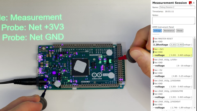
The real-life highlighting of components is achieved thanks to a set of cameras that track the motion of everything on the desk as well as a video projector that overlays information on top of the PCB. All of this enables a variety of useful debugging features: for example, there’s an option to highlight pin one on all components, enabling a simple visual check of each component’s orientation. You can select all Do Not Populate (DNP) instances and immediately see if all highlighted pads are empty. If you’re not sure which component you’re looking at, just point at it with your multimeter probe and it’s highlighted on the schematic and layout. You can even place your probes on a net and automatically log the voltage for future reference, thanks to a digital link between the multimeter and the ARDW software.
In addition to designing and building the ARDW, the team also performed a usability study using a group of human test subjects. They especially liked the ability to quickly locate components on crowded boards, but found the on-line measurement system a bit cumbersome due to its limited positional accuracy. Future work will therefore focus on improving the resolution of the projected image and generally making the system more compact and robust. All software is freely available on the project’s GitHub page, and while the current system looks a little complex for hobbyist use, we can already imagine it being a useful tool in production environments.
It’s not even the first time augmented reality has been used for PCB debugging: we saw a somewhat similar system at the 2019 Hackaday Superconference. AR can also come in handy during the design and prototyping phase, as demonstrated by this AR breadboard.


Really cool idea, hope to see a version that requires less supporting hardware in the future
I think their goal was to show the application idea, so they went for the best possible setup to be able to focus on the bit they really care about, not the tracking setup.
This should be doable with a decent camera, cheap projector and a bit of setup/calibration to align the two. But it would be more finicky than the high end setup they have there – e.g. when a hand or a probe occludes the board the tracking could be lost if you have only a single camera. The same if the only camera gets a glare from the board, etc.
But an integrated, low cost setup using e.g. a few webcams (or RPi cameras!) + a cheap LED projector could be in the realm of possibility. The tracking and projector parts are well known and solved problems, not requiring any crazy complex solutions.
The main part that would make or break this wouldn’t be the hardware but the application software, though. The calibration would need to be quick and simple, tracking robust and the interaction with the board and software really robust and frictionless, so that I wouldn’t need to futz with some settings constantly or have to put the probes/iron/tweezers down to hunt for the mouse to adjust this or change that.
Instead of a projector shining picture to the table, you could just show the whole thing on a screen.
This would help achieve Olivier’s request outlined about, only need a camera aimed at the bench at that point
Which would completely miss the point of the augmentations. If you have to take your eyes off the board and probes to look at the screen, you can as well ditch the entire setup and just look up the schematic/board layout directly. There is board view software that does exactly that already.
No it does not. You look at the screen, it shows the camera image of the board with the augmented stuff.
It’s not hard to look at the screen and direct your hands where you need to probe.
I like the heads up display on the workbench.
Now add Volt/Current readings and oscilloscope display to the heads up on the work bench.
I think this project is AWESOME!
You can probably drop the need for the tracking of the probes and then get by with only a board-level track and overhead projector display. I personally would be OK with that, and it’d be much more feasible.
The probe tracked selections and measurements are a nice bonus, but…
Let’s be honest. How much better would it be to manually assemble PCBs with that highlighting??
Let’s hope the developers wrote the software stack modularly enough to remove the 3D probe track and only use the board track.
Cool! I was actually going to be in user testing for this project, but the scheduling didn’t work out and I had to cancel. I’m happy to learn what I missed.
InspectAR.com does this with your phone. I think it’s owned by Digi-Key.
room for improvement
https://hackaday.com/2020/04/03/oscilloscope-and-microscope-augmented-with-ghosts/
I had this idea 5-6years ago and posted it. So I hope it is not possible to patent it anymore. :-)
But it is necessary to do this with a microscope, because in this days 90% of my work happens
with a microscope. And the next step is a standard for all manufacturer of measurement devices. So it is easily possible to show there values in the 3D-microscope picture.
Olaf
I did a video on a very rough & basic version of this a few years ago: https://youtu.be/QHW3LFHhiJM
It was meant as a guide for assembly and repair, not as much for measurement.
i don’t think probing the board under test on an antistatic mat is a good idea.
at best its too easy to get wonky values due to the path to gnd
Very cool project and love the work the University of Washington has been doing, especially the way this leverages the iBOM plugin for KiCAD that is one of the coolest user experiences I have seen for in lab debugging.
The motion capture stuff for taking measurements is really novel, never seen that done in a PCBA use case before hats off to the team here :)
Nice
Very nice indeed, but if users are complaining about poor alignment then they need to use telecentric lenses to prevent the height of the component above the work surface being an issue.