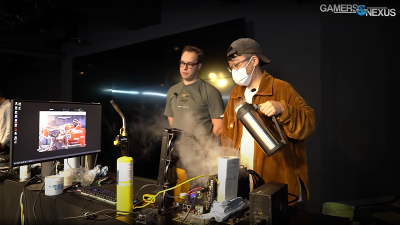
It’s not news that EVGA is getting out of the GPU card game, after a ‘little falling out’ with Nvidia. It’s sad news nonetheless, as this enthusiastic band of hardware hackers has a solid following in certain overclocking and custom PC circles. The Games Nexus gang decided to fly over to meet up with the EVGA team in Zhonghe, Taiwan, and follow them around a bit as they tried for one last overclocking record on the latest (unreleased, GTX4090-based) GPU card. As you will note early on in the video, things didn’t go smoothly, with their hand-lapped GPU burning out the PCB after a small setup error.
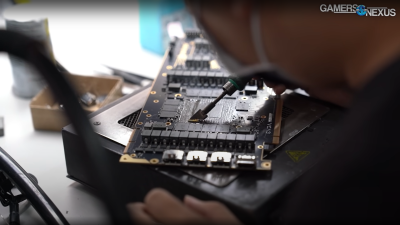
The fun parts of the video show some behind-the-scenes details of the EVGA GPU operation, including some sections of BGA reworking which are pretty informative (but we’d like more detail, thanks!) showing that even with only a handful of AD102 Silicon available and a few prototype PCBs, even letting out the magic smoke is not necessarily the end of the show.
But why hand-lap the die? Apparently, the surface is pre-curved outwards, so that when it warms up under load, the die surface ends up flat, making the best contact with the thermal interface surface of the cooler. But [biso biso] uses liquid nitrogen for their overclocking speed records, and that has the opposite effect, with the extreme cooling (about -90 Celsius) causing the die to flex differently, and ‘crack’ the thermal paste, ruining the thermal contact with the cooling media. Lapping the die back to flat, apparently reduces this problem.
On the rework side of things, (14:45 in the video) they needed to remove the lapped GPU from the blown card using a standard IR rework station. The technician waited for the moment all the GPU balls were molten, before quickly whipping away the smoking chip with a vacuum pickup. Next, it was thoroughly cleaned and brushed with flux whilst sitting on a preheater. After hand-tinning the pads, it’s ready for the re-balling jig, and given a sprinkling of fresh balls, before a trip through the oven to fix them in place. Finally, after ultrasonic cleaning, it was ready for testing on a socketed development card. Once a test pass was achieved, the GPU was mounted onto a suitably prepared donor PCB, likely using the same reflow station seen earlier (but that was not shown,) it’s a simple process, but a skilled one that the repair team does all the time, making it look effortless. We’d sure break a sweat trying to do this!
Think all this PC overclocking, just for a short-lived record is somewhat pointless? How about an overclocked TI-84 instead?
And, an earlier video with a tour of the EVGA shop:
Thanks to [Simon] for the tip!


I owned an EVGA video card.
Very average copy of a NVIDEA ref board, died young. They were on the ‘never again’ list.
‘Nothing of value was lost.’
On the flip side, I’ve used almost nothing but EVGA cards for Folding@Home, my current pair having survived the previous AZ summer in the garage, and currently keeping said garage at 60˚F during the winter.
Welcome to being the 0.000000001% of people. lmao
That’s only equivalent to the left leg of one person! A few too many zeros, me thinks.
PC Partner. You owned a PC Partner developed and fabricated board with an EVGA brand cooler / logo. Built to Nvidia’s specs and just as reliable as their fix it in post white sheets.
Seriously EVGA and several other GPU manufacturers are technically fab less GPU manufacturers. They do roll their own stuff when it suits them but they basically use companies like PC Partner to make the OG stuff and then tweak. Sapphire the long fabled AMD “reference” designer uses… drum roll please…. PC Partner.
“Seriously EVGA and several other GPU manufacturers are technically fab less GPU manufacturers.” No…
EVGA, Asus, gigabyte, Sapphire, etc. Are all “Add in board” partners.
Ie, they don’t make the graphics processing unit. But rather design and manufacture a board to house it on and provide it with power, not to mention the cooler.
AMD and nVidia do make reference designs for these manufacturers to base their own designs on. And also to help them get the first products to market in time.
Also. “PC Partner. You owned a PC Partner developed and fabricated board with an EVGA brand cooler / logo.”
Is odd, considering that EVGA isn’t (and has never been) a subsidiary of PC Partner. (Sapphire meanwhile is a subsidiary of PC Partner.) So it wouldn’t be in PC Partner’s interests to manufacture things for EVGA.
Secondly, it would be even more odd for EVGA to have a whole graphics card design department if they relied on PC Partner for the design part of the product.
It’s worth noting that EVGA weren’t “just” GPU manufacturers.
The were constantly fighting to get around Nvidia’s bullshit restrictions.
These restrictions were NOT there for any pro-consumer reasons. They were purely based around squeezing the most pennies from the most people.
The things EVGA were able to do pushed the ENTIRE GPU market forward, even if you had nothing to do with overclocking or breaking limits.
EVGA leaving the GPU market is just one less Lego on the floor that can slow Nvidia down.
I rarely have anything good to say about a corporation, but EVGA was pretty decent. And Nvidia’s behavior in this is a perfect example of the evils of ultra-capitalism.
When your customers are the shareholders, your business becomes “make money number bigger at all costs”.
“When your customers are the shareholders, your business becomes “make money number bigger at all costs”.”
Which is US with a capital “U”.
You are low quality, if you watched the video, which you didn’t, you would realised how cool this article is.
Cryogenic, I would say.
So says the disgruntled Nvidia employee. :D
“GamersNexus” not “Gamer Nexus”. Don’t let Steve from GN find out!